This paper demonstrates that dielectric nano-antennas can induce significant strain in atomically thin WSe$_2$ layers, modifying their optical properties. Strain up to 1.4% in monolayers and >3% in bilayers is achieved, leading to direct bandgap formation and exciton confinement, enhancing photoluminescence and showing potential for engineering light-matter interactions in nano-photonic devices.
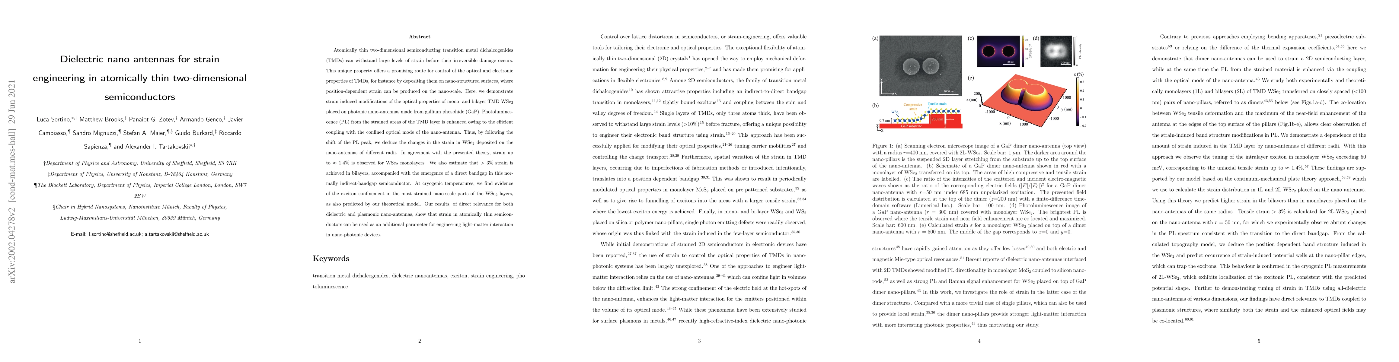
Atomically thin two-dimensional semiconducting transition metal dichalcogenides (TMDs) can withstand large levels of strain before their irreversible damage occurs. This unique property offers a promising route for control of the optical and electronic properties of TMDs, for instance by depositing them on nano-structured surfaces, where position-dependent strain can be produced on the nano-scale. Here, we demonstrate strain-induced modifications of the optical properties of mono- and bilayer TMD WSe$_2 $ placed on photonic nano-antennas made from gallium phosphide (GaP). Photoluminescence (PL) from the strained areas of the TMD layer is enhanced owing to the efficient coupling with the confined optical mode of the nano-antenna. Thus, by following the shift of the PL peak, we deduce the changes in the strain in WSe$_2$ deposited on the nano-antennas of different radii. In agreement with the presented theory, strain up to $\approx 1.4 \%$ is observed for WSe$_2$ monolayers. We also estimate that $>3\%$ strain is achieved in bilayers, accompanied with the emergence of a direct bandgap in this normally indirect-bandgap semiconductor. At cryogenic temperatures, we find evidence of the exciton confinement in the most strained nano-scale parts of the WSe$_2$ layers, as also predicted by our theoretical model. Our results, of direct relevance for both dielectric and plasmonic nano-antennas, show that strain in atomically thin semiconductors can be used as an additional parameter for engineering light-matter interaction in nano-photonic devices.
This graph shows how this paper is connected to other research. The current paper is shown in dark gray, papers that cite it are in green, and papers it references are in blue. You can:
• Hover over any node to see the paper title
• Click a node to view that paper's details
• Drag nodes to rearrange the graph
• Use the zoom controls (bottom right) to zoom in/out
Title | Authors | Year | Actions |
---|---|---|---|
Chiral Nonlinear Polaritonics with van der Waals Metasurfaces
|
Connor Heimig, A. Antonov, Dmytro Gryb, Thomas Possmayer, Thomas Weber, Michael Hirler, Jonas Biechteler, Luca Sortino, L. D. S. Menezes, Stefan A. Maier, M. Gorkunov, Y. Kivshar, A. Tittl
|
2024
|
View Paper |
Valleytronics Meets Straintronics: Valley Fine Structure Engineering of 2D Transition Metal Dichalcogenides
|
Shichao Yang, Hanyan Long, Wenwei Chen, Baisheng Sa, Zhiyong Guo, Jingying Zheng, Jiajie Pei, Hongbing Zhan, Yuerui Lu
|
2024
|
View Paper |
Single-emitter super-resolved imaging of radiative decay rate enhancement in dielectric gap nanoantennas
|
R. M. Córdova-Castro, B. van Dam, A. Lauri, Stefan A. Maier, Riccardo Sapienza, Y. De Wilde, I. Izeddin, V. Krachmalnicoff
|
2024
|
View Paper |
Layer-number and strain effects on the structural and electronic properties of PtSe2material.
|
Rania Amairi, Adlen Smiri, Sihem Jaziri
|
2023
|
View Paper |
Photoluminescence Enhancement of Monolayer WS2 by n-Doping with an Optically Excited Gold Disk
|
Bayarjargal N Tugchin, Nathan Doolaard, Ángela I Barreda, Zifei Zhang, Anastasia Romashkina, S. Fasold, I. Staude, Falk Eilenberger, Thomas Pertsch
|
2023
|
View Paper |
Photosensitizing Metasurface Empowered by Enhanced Magnetic Field of Toroidal Dipole Resonance.
|
H. Hasebe, H. Sugimoto, Y. Katsurayama, Taniyuki Furuyama, M. Fujii
|
2023
|
View Paper |
Radiative suppression of exciton–exciton annihilation in a two-dimensional semiconductor
|
Luca Sortino, Merve Gülmüs, Benjamin Tilmann, L. de S. Menezes, S. A. Maier
|
2023
|
View Paper |
Gallium Phosphide Nanoparticles for Low‐Loss Nanoantennas in Visible Range
|
Daisuke Shima, H. Sugimoto, A. Assadillayev, S. Raza, M. Fujii
|
2023
|
View Paper |
Crested 2D materials for optoelectronics and photonics
|
Siwei Luo, Gencai Guo, X. Qi, Weiyang Liu, Han Tang, Q. Bao, Jianxin Zhong
|
2022
|
View Paper |
Van der Waals Materials for Applications in Nanophotonics
|
Panaiot G. Zotev, Yue Wang, D. Andres-Penares, Toby Severs‐Millard, S. Randerson, Xuerong Hu, Luca Sortino, Charalambos Louca, M. Brotons-Gisbert, T. Huq, S. Vezzoli, R. Sapienza, T. Krauss, B. Gerardot, A. Tartakovskii
|
2022
|
View Paper |
Optical Metasurfaces for Energy Conversion
|
E. Cortes, F. Wendisch, Luca Sortino, A. Mancini, S. Ezendam, Seryio Saris, L. de S. Menezes, Andreas Tittl, H. Ren, S. A. Maier
|
2022
|
View Paper |
Electron Dynamics in a Two-Dimensional Nanobubble: A Two-Level System Based on Spatial Density.
|
R. Rosati, F. Lengers, C. Carmesin, M. Florian, T. Kuhn, F. Jahnke, M. Lorke, D. Reiter
|
2021
|
View Paper |
Plasmon damping and charge transfer pathways in Au@MoSe2 nanostructures
|
I. Abid, P. Benzo, B. Pécassou, S. Jia, Jing Zhang, Jiangtan Yuan, J. B. Dory, O. G. Lafaye, R. Péchou, A. Mlayah, Jun Lou
|
2021
|
View Paper |
Engineered near- and far-field optical response of dielectric nanostructures using focused cylindrical vector beams
|
Martin Montagnac, G. Agez, Adelin Patoux, A. Arbouet, Vincent Paillard
|
2021
|
View Paper |
Strained MoSi2N4 Monolayers with Excellent Solar Energy Absorption and Carrier Transport Properties
|
Chao-chao Jian, Xiangchao Ma, Jianqi Zhang, Xin Yong
|
2021
|
View Paper |
Strain-tuning of the electronic, optical, and vibrational properties of two-dimensional crystals
|
E. Blundo, E. Cappelluti, M. Felici, G. Pettinari, A. Polimeni
|
2021
|
View Paper |
Transition Metal Dichalcogenide Dimer Nanoantennas for Tailored Light–Matter Interactions
|
Panaiot G. Zotev, Yue Wang, Luca Sortino, Toby Severs Millard, N. Mullin, D. Conteduca, Mostafa Shagar, A. Genco, J. Hobbs, T. Krauss, A. Tartakovskii
|
2021
|
View Paper |
Bright single photon emitters with enhanced quantum efficiency in a two-dimensional semiconductor coupled with dielectric nano-antennas
|
Luca Sortino, Panaiot G. Zotev, C. L. Phillips, A. Brash, J. Cambiasso, Elena Marensi, A. M. Fox, S. Maier, R. Sapienza, A. Tartakovskii
|
2021
|
View Paper |
Unveiling the Optical Emission Channels of Monolayer Semiconductors Coupled to Silicon Nanoantennas
|
J. Poumirol, I. Paradisanos, S. Shree, G. Agez, X. Marie, C. Robert, N. Mallet, Peter R. Wiecha, G. Larrieu, V. Larrey, F. Fournel, Kenji Watanabe, T. Taniguchi, A. Cuche, V. Paillard, B. Urbaszek
|
2020
|
View Paper |
Exciton Diffusion and Annihilation in Nanophotonic Purcell Landscapes
|
T. V. Raziman, C. Peter Visser, Shaojun Wang, Jaime Gómez Rivas, A. Curto
|
2020
|
View Paper |
Recent Advances in Strain-Induced Piezoelectric and Piezoresistive Effect-Engineered 2D Semiconductors for Adaptive Electronics and Optoelectronics
|
Feng Li, Tao Shen, Cong Wang, Yupeng Zhang, J. Qi, Han Zhang
|
2020
|
View Paper |
Published: 2019-11-12
Published: 2021-10-20
Comments (0)