Publication
Metrics
Paper Preview
Abstract
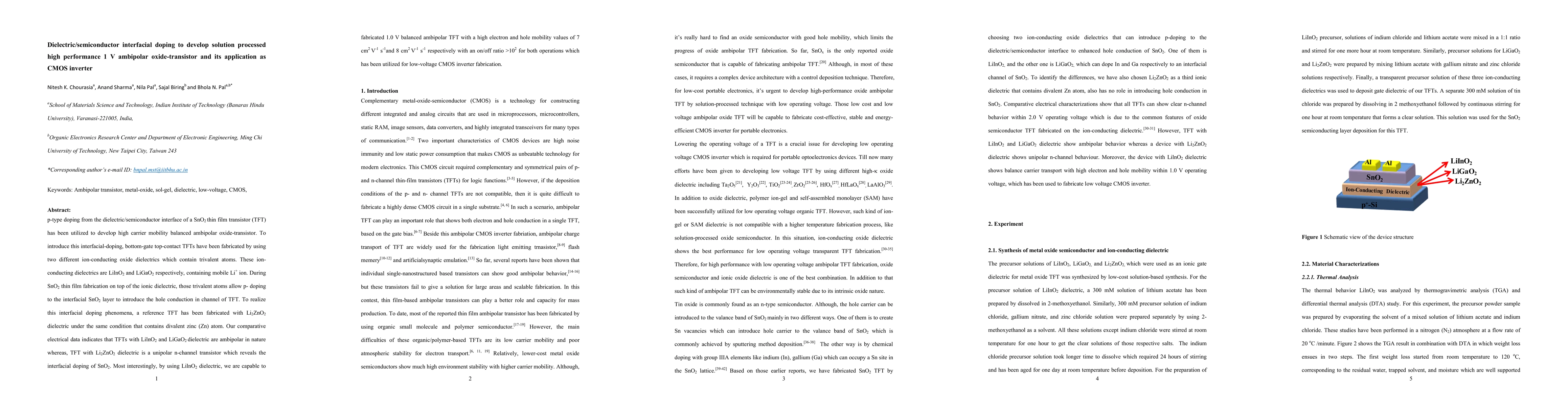
p-type doping from the dielectric/semiconductor interface of a SnO2 thin film transistor (TFT) has been utilized to develop high carrier mobility balanced ambipolar oxide-transistor. To introduce this interfacial-doping, bottom-gate top-contact TFTs have been fabricated by using two different ion-conducting oxide dielectrics which contain trivalent atoms. These ion-conducting dielectrics are LilnO2 and LiGaO2 respectively, containing mobile Li+ ion. During SnO2 thin film fabrication on top of the ionic dielectric, those trivalent atoms allow p- doping to the interfacial SnO2 layer to introduce the hole conduction in channel of TFT. To realize this interfacial doping phenomena, a reference TFT has been fabricated with Li2ZnO2 dielectric under the same condition that contains divalent zinc (Zn) atom. Our comparative electrical data indicates that TFTs with LilnO2 and LiGaO2 dielectric are ambipolar in nature whereas, TFT with Li2ZnO2 dielectric is a unipolar n-channel transistor which reveals the interfacial doping of SnO2. Most interestingly, by using LilnO2 dielectric, we are capable to fabricated 1.0 V balanced ambipolar TFT with a high electron and hole mobility values of 7 cm2 V-1 s-1and 8 cm2 V-1 s-1 respectively with an on/off ratio >102 for both operations which has been utilized for low-voltage CMOS inverter fabrication.
AI Key Findings
Get AI-generated insights about this paper's methodology, results, significance, and more — seven facets brought into focus.
Paper Details
Authors
PDF Preview
Key Terms
Related Papers
No references found for this paper.
Discussion 0