Researchers developed a model to predict nanopatterning in alloys during ion sputtering, which successfully reproduced experimentally observed structures. The study also found that segregation plays a key role in the pattern-formation process.
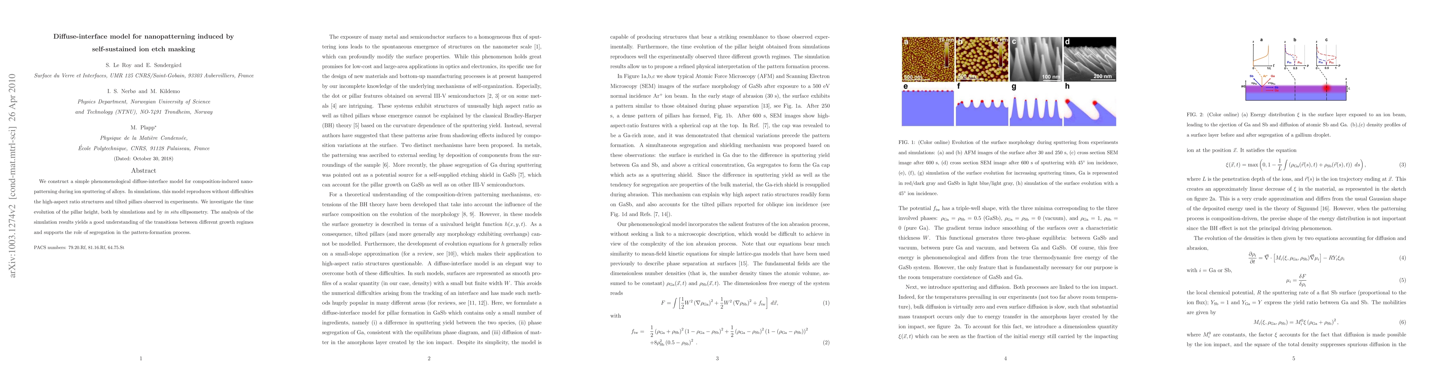
We construct a simple phenomenological diffuse-interface model for composition-induced nanopatterning during ion sputtering of alloys. In simulations, this model reproduces without difficulties the high-aspect ratio structures and tilted pillars observed in experiments. We investigate the time evolution of the pillar height, both by simulations and by {\it in situ} ellipsometry. The analysis of the simulation results yields a good understanding of the transitions between different growth regimes and supports the role of segregation in the pattern-formation process.
Get AI-generated insights about this paper's methodology, results, and significance.
Current paper (gray), citations (green), references (blue)
Title | Authors | Year | Actions |
---|---|---|---|
An in situ real-time growth study of Ag film on the ion beam sculptured GaSb nanostructures
|
Praveen Kumar Dubey, Sarath Sasi, Kumar Navin, Benedikt Sochor, Stephan V. Roth, P.S. Anil Kumar, Ajay Gupta, S. K. Vayalil
|
2025
|
View Paper |
Phase-field model of glass transition: behavior under uniform quenching
|
M. Vasin, Vladimir Ankudinov
|
2024
|
View Paper |
Dynamics of nanoscale triangular features on Ge surfaces
|
Sukriti Hans, B. K. Parida, Vivek Pachchigar, S. Augustine, Sooraj Kp, M. Ranjan
|
2022
|
View Paper |
Surface nanopatterning by ion beam irradiation: compositional effects
|
L. Vázquez, A. Redondo-Cubero, K. Lorenz, F. J. Palomares, R. Cuerno
|
2022
|
View Paper |
Soft model of solidification with the order–disorder states competition
|
M. Vasin, V. Ankudinov
|
2021
|
View Paper |
Anisotropic electrical conduction on ion induced nanorippled CoSi surface
|
B. K. Parida, A. Kundu, K. Hazra, S. Sarkar
|
2021
|
View Paper |
Nanopatterning of the (001) surface of crystalline Ge by ion irradiation at off-normal incidence: Experiment and simulation
|
D. Erb, Ricardo de Schultz, A. Ilinov, K. Nordlund, R. M. Bradley, S. Facsko
|
2020
|
View Paper |
Nonlinear compositional and morphological evolution of ion irradiated GaSb prior to nanostructure formation
|
Michael A. Lively, B. Holybee, Michael Y. Toriyama, S. Facsko, J. Allain
|
2020
|
View Paper |
Stoichiometric influences on ion beam nanopatterning of CoSi binary compound
|
B. K. Parida, S. Sarkar
|
2020
|
View Paper |
Ion-induced nanopatterning of silicon: Toward a predictive model
|
S. Norris, M. Aziz
|
2019
|
View Paper |
Tilted InSb nanostructures fabricated by off-normal ion beam irradiation
|
S. Yamashita, T. Oishi, T. Miyaji, C. Watanabe, N. Nitta
|
2018
|
View Paper |
Recent developments in ion beam-induced nanostructures on AIII-BV compound semiconductors
|
E. Trynkiewicz, B. Jany, A. Janas, F. Krok
|
2018
|
View Paper |
Massive-scale molecular dynamics of ion-irradiated III–V compound semiconductors at the onset of nanopatterning
|
Michael A. Lively, B. Holybee, Michael Y. Toriyama, J. Allain
|
2017
|
View Paper |
Unraveling atomic-level self-organization at the plasma-material interface
|
J. Allain, A. Shetty
|
2017
|
View Paper |
Plasma fireball: A unique tool to fabricate patterned nanodots.
|
S. Chauhan, T. Barman, M. Bhatnagar, M. Ranjan, S. Mukherjee
|
2017
|
View Paper |
Novel analytical method for investigating compositional driven ion-induced nanopatterning of multicomponent materials
|
B. Holybee
|
2016
|
View Paper |
Utilizing Neon Ion Microscope for GaSb nanopatterning studies: Nanostructure formation and comparison with low energy nanopatterning
|
O. El-Atwani, C. Huynh, S. Norris
|
2016
|
View Paper |
Ion beam nanopatterning of III-V semiconductors: consistency of experimental and simulation trends within a chemistry-driven theory
|
O. El-Atwani, Scott A. Norris, Karl F. Ludwig, S. Gonderman, Jean Paul Allain, Jean Paul Allain
|
2015
|
View Paper |
Energy dependence of nanopillars formation on InSb semiconductor surfaces under gallium FIB and noble gas ions beam irradiation
|
B. Jany, K. Szajna, M. Nikiel, D. Wrana, E. Trynkiewicz, R. Pȩdrys, F. Krok
|
2015
|
View Paper |
Self-organized nanopatterning of silicon surfaces by ion beam sputtering
|
J. Muñoz-García, L. Vázquez, M. Castro, R. Gago, A. Redondo-Cubero, A. Moreno-Barrado, R. Cuerno
|
2014
|
View Paper |
Combining surface X-ray scattering and ellipsometry for non-destructive characterization of ion beam-induced GaSb surface nanostructures
|
Kristin Høydalsvik, L. M. S. Aas, Ellen Døli, E. Søndergård, M. Kildemo, D. Breiby
|
2014
|
View Paper |
The role of metal layers in the formation of metal-silicon hybrid nanoneedle arrays.
|
Hai Liu, C. Khoo, Boluo Yadian, Qing Liu, C. Gan, X. Tang, Yizhong Huang
|
2014
|
View Paper |
Nanoscale compositional banding in binary thin films produced by ion-assisted deposition
|
R. M. Bradley
|
2013
|
View Paper |
Ion-assisted phase separation in compound films: An alternate route to ordered nanostructures
|
S. Norris
|
2013
|
View Paper |
Unifying binary fluid diffuse-interface models in the sharp-interface limit
|
D. Sibley, A. Nold, S. Kalliadasis
|
2013
|
View Paper |
Near sputter-threshold GaSb nanopatterning
|
O. El-Atwani, S. Gonderman, J. Allain
|
2013
|
View Paper |
Ion-induced roughening and ripple formation on polycrystalline metallic films
|
T. Škereň, K. Temst, W. Vandervorst, A. Vantomme
|
2013
|
View Paper |
Determination of small tilt angles of short GaSb nanopillars using UV–visible Mueller matrix ellipsometry
|
L. M. Aas, M. Kildemo, Y. Cohin, E. Søndergård
|
2013
|
View Paper |
Non-antireflective scheme for efficiency enhancement of Cu(In,Ga)Se2 nanotip array solar cells.
|
Y. Liao, Yi‐Chung Wang, Yu-Ting Yen, Chia-Hsiang Chen, D. Hsieh, Shih-Chen Chen, Chia-Yu Lee, Chih-chung Lai, Wei-Chen Kuo, J. Juang, Kaung-Hsiung Wu, Shun-Jen Cheng, C. Lai, F. Lai, S. Kuo, H. Kuo, Y. Chueh
|
2013
|
View Paper |
Selbstorganisierte Nanostrukturen auf Germanium und Galliumantimonid und ihre Nutzung als Template
|
M. Fritzsche
|
2013
|
View Paper |
Ageing dynamics of ion bombardment induced self-organization processes
|
O. Bikondoa, D. Carbone, V. Chamard, T. Metzger
|
2013
|
View Paper |
Nanopatterning of metal-coated silicon surfaces via ion beam irradiation: Real time x-ray studies reveal the effect of silicide bonding
|
O. El-Atwani, S. Gonderman, A. Demasi, A. Suslova, J. Fowler, Mohamad El-Atwani, K. Ludwig, J. Allain
|
2013
|
View Paper |
Crater functions for compound materials: A route to parameter estimation in coupled-PDE models of ion bombardment
|
S. Norris, J. Samela, Matias Vestberg, K. Nordlund, M. Aziz
|
2013
|
View Paper |
Real time x-ray studies during nanostructure formation on silicon via low energy ion beam irradiation using ultrathin iron films
|
Anastassiya Suslova, Alexander DeMasi, S. Gonderman, J. Fowler, Mohamad El-Atwani, K. Ludwig, J. Allain
|
2012
|
View Paper |
The effect of native oxide on ion-sputtering-induced nanostructure formation on GaSb surfaces
|
O. El-Atwani, J. Allain, A. Suslova
|
2012
|
View Paper |
- Low-Energy Ion-Induced Pattern Formation in Si-Ge Alloy
|
A. Sarkar
|
2012
|
View Paper |
Surface Nanopatterns on Si(100) by Normal-Incidence Ion Sputtering with Metal Incorporation
|
R. Gago, J. A. Sánchez-García, A. Redondo-Cubero, L. Vázquez
|
2012
|
View Paper |
A Unified Spatio-Temporal Framework of the Cuerno—Barabasi Stochastic Continuum Model of Surface Sputtering
|
O. Oyewande
|
2012
|
View Paper |
Phase separation in ion-irradiated compound semiconductors: an alternate route to ordered nano-structures
|
S. Norris
|
2012
|
View Paper |
A chemically-driven finite-wavelength instability in ion-irradiated compound semiconductors
|
S. Norris
|
2012
|
View Paper |
Hydrodynamic approach to surface pattern formation by ion beams
|
M. Castro, R. Cuerno
|
2011
|
View Paper |
The significance of in situ conditions in the characterization of GaSb nanopatterned surfaces via ion beam sputtering
|
O. El-Atwani, J. Allain, A. Cimaroli, A. Suslova, Sami Ortoleva
|
2011
|
View Paper |
Focused ion beam creation and templating of InAs and InAs/InP nanospikes
|
Kevin A. Grossklaus, J. Millunchick
|
2011
|
View Paper |
Theory of nanoscale pattern formation induced by normal-incidence ion bombardment of binary compounds
|
Patrick D. Shipman, R. M. Bradley
|
2011
|
View Paper |
Real-time in situ Mueller matrix ellipsometry of GaSb nanopillars: observation of anisotropic local alignment.
|
I. S. Nerbø, S. Le Roy, M. Foldyna, E. Søndergård, M. Kildemo
|
2011
|
View Paper |
Thermally controlled growth of surface nanostructures on ion-modified AIII-BV semiconductor crystals
|
E. Trynkiewicz, B. Jany, D. Wrana, F. Krok
|
2018
|
View Paper |
Real-time Study of the Formation of GaSb Nanopillars by Spectroscopic Mueller Matrix Ellipsometry
|
I. S. Nerbø
|
2011
|
View Paper |
Comments (0)