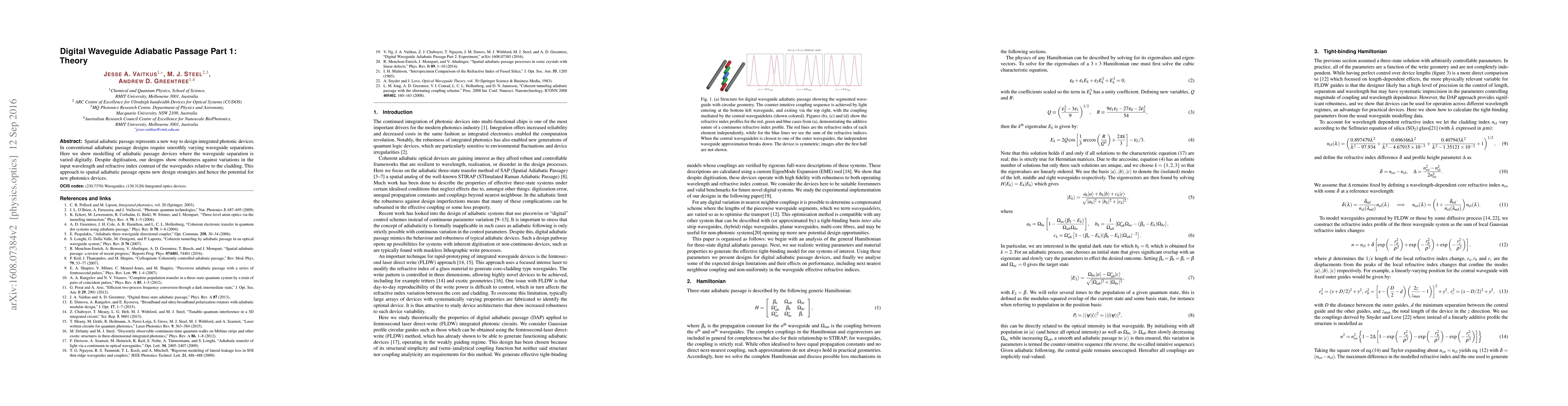
Publication
Metrics
AI Quick Summary
This paper introduces the theory behind digital waveguide adiabatic passage for integrated photonic devices, demonstrating robust design strategies despite digital waveguide separation variations. This novel approach offers new design possibilities for advanced photonics applications.
Paper Preview
Abstract
Spatial adiabatic passage represents a new way to design integrated photonic devices. In conventional adiabatic passage designs require smoothly varying waveguide separations. Here we show modelling of adiabatic passage devices where the waveguide separation is varied digitally. Despite digitisation, our designs show robustness against variations in the input wavelength and refractive index contrast of the waveguides relative to the cladding. This approach to spatial adiabatic passage opens new design strategies and hence the potential for new photonics devices.
AI Key Findings
Get AI-generated insights about this paper's methodology, results, significance, and more — seven facets brought into focus.
Impact
Paper Details
PDF Preview
Key Terms
Citation Network
Current paper (gray), citations (green), references (blue)
Display is limited for performance on very large graphs.
Discussion 0