ArxivLens
ArXiv physics.optics physics.app-ph

Digitized Adjoint Method for Inverse Design of Digital Nanophotonic Devices

1902.00654 Published Feb 5, 2019
View PDF

Publication

Published: Feb 05, 2019
Categories: physics.optics, physics.app-ph

Metrics

Source: ArXiv

AI Quick Summary

The paper introduces a digitized adjoint method for efficient inverse design of subwavelength nanophotonic devices, demonstrating its application in optimizing a single-mode 3-dB power divider and a dual-mode demultiplexer. This method significantly enhances design efficiency by about five times compared to brute-force methods, leveraging multi-level digital patterns for improved performance.

Quick Answers

What is "Digitized Adjoint Method for Inverse Design of Digital Nanophotonic Devices" about?

The paper introduces a digitized adjoint method for efficient inverse design of subwavelength nanophotonic devices, demonstrating its application in optimizing a single-mode 3-dB power divider and a dual-mode demultiplexer. This method significantly enhances design efficiency by about five times compared to brute-force methods, leveraging multi-level digital patterns for improved performance.

What methodology did the authors use?

The research presents a digitized adjoint method combining adjoint sensitivity analysis with digital subwavelength structures for inverse design of compact nanophotonic devices, involving three stages: continuous variation, forced permittivity biasing, and multi-level digital pattern transformation. More in Methodology →

What are the key results?

The digitized adjoint method improves design efficiency by approximately 5 times compared to the conventional brute-force method. — Performance optimization reaches a similar level using a ternary pattern (N = 3) compared to continuous patterns. More in Key Results →

Why is this work significant?

This research offers a novel approach to overcome the efficiency bottleneck of brute-force methods in designing large-scale digital nanophotonic devices, potentially enabling the creation of devices with enhanced performance and functionality. More in Significance →

What are the main limitations?

The method relies on specific simulation software (Lumerical FDTD Solutions) and computational resources (8-core CPU, 64 GB memory). — Experimental validation was conducted only for two device types, limiting the generalizability of results. More in Limitations →

Paper Preview

Abstract

We present a digitized adjoint method for realizing efficient inverse design of "digital" subwavelength nanophotonic devices. We design a single-mode 3-dB 
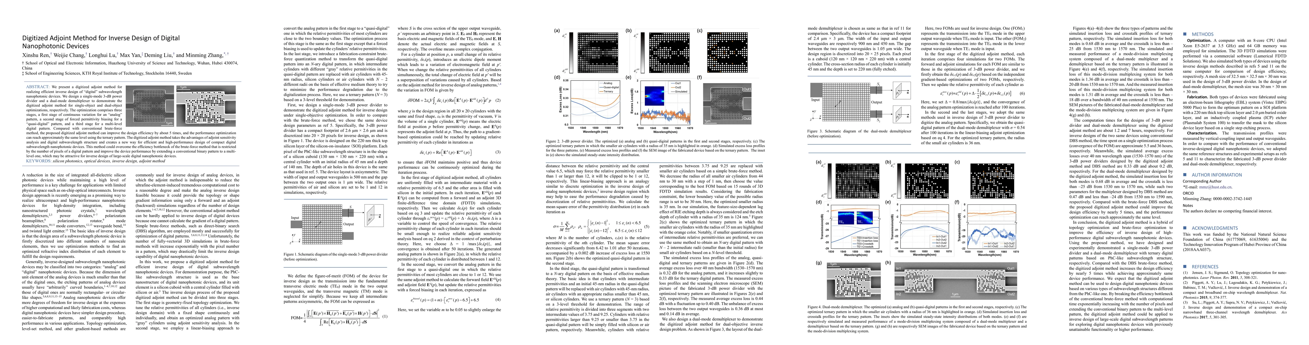
power divider and a dual-mode demultiplexer to demonstrate the digitized adjoint method for single-object and dual-object optimizations, respectively. The optimization comprises three stages, a first stage of continuous variation for an "analog" pattern, a second stage of forced permittivity biasing for a "quasi-digital" pattern, and a third stage for a multi-level digital pattern. Compared with conventional brute-force method, the proposed digitized adjoint method can improve the design efficiency by about 5 times, and the performance optimization can reach approximately the same level using the ternary pattern. The digitized adjoint method takes the advantages of adjoint sensitivity analysis and digital subwavelength structure and creates a new way for efficient and high-performance design of compact digital subwavelength nanophotonic devices. This method could overcome the efficiency bottleneck of the brute-force method that is restricted by the number of pixels of a digital pattern and improve the device performance by extending a conventional binary pattern to a multi-level one, which may be attractive for inverse design of large-scale digital nanophotonic devices.

Key Findings, in focus

Seven facets of this paper, analysed and brought into focus by AI.

AI-generated · verify against source Generated Sep 02, 2025
In focus · one-line synthesis

This research offers a novel approach to overcome the efficiency bottleneck of brute-force methods in designing large-scale digital nanophotonic devices, potentially enabling the creation of devices with enhanced performance and functionality.

01
MethodologyHow they did it

The research presents a digitized adjoint method combining adjoint sensitivity analysis with digital subwavelength structures for inverse design of compact nanophotonic devices, involving three stages: continuous variation, forced permittivity biasing, and multi-level digital pattern transformation.

02
ResultsWhat they found
  • The digitized adjoint method improves design efficiency by approximately 5 times compared to the conventional brute-force method.
  • Performance optimization reaches a similar level using a ternary pattern (N = 3) compared to continuous patterns.
  • The method successfully designed a single-mode 3-dB power divider and a dual-mode demultiplexer with ternary digital patterns.
  • Measured performance of fabricated devices aligns well with simulated results, demonstrating the method's practicality.
03
SignificanceWhy it matters

This research offers a novel approach to overcome the efficiency bottleneck of brute-force methods in designing large-scale digital nanophotonic devices, potentially enabling the creation of devices with enhanced performance and functionality.

04
Technical ContributionsWhat's new technically

The digitized adjoint method integrates adjoint sensitivity analysis with digital pattern optimization, creating a hybrid approach that enhances design efficiency for nanophotonic devices.

05
NoveltyWhat sets it apart

The proposed method combines topology optimization and brute-force optimization, breaking the computational time dependency on the number of pixels and extending binary patterns to multi-level ones, which sets it apart from existing inverse design methods.

06
LimitationsWhat to be cautious about
  • The method relies on specific simulation software (Lumerical FDTD Solutions) and computational resources (8-core CPU, 64 GB memory).
  • Experimental validation was conducted only for two device types, limiting the generalizability of results.
07
Future WorkWhere it goes next
  • Explore the applicability of the digitized adjoint method to various subwavelength structures beyond PhC-like designs.
  • Investigate the method's performance and efficiency for designing more complex nanophotonic devices.

Impact

15
References
1
Influential

Paper Details

Paper ID: 1902.00654
License: http://arxiv.org/licenses/nonexclusive-distrib/1.0/
Categories:
physics.optics physics.app-ph

How to Cite This Paper

Reference manager: RIS EndNote

Key Terms

adjoint (0.306)
digital (0.292)
pattern (0.275)
multi level (0.214)
stage (0.209)
design (0.187)
devices (0.181)
force (0.156)

Citation Network

Current paper (gray), citations (green), references (blue)

Display is limited for performance on very large graphs.

Current Paper
Citations
References
Click to view


Discussion 0

This website uses cookies to ensure you get the best experience. Learn more