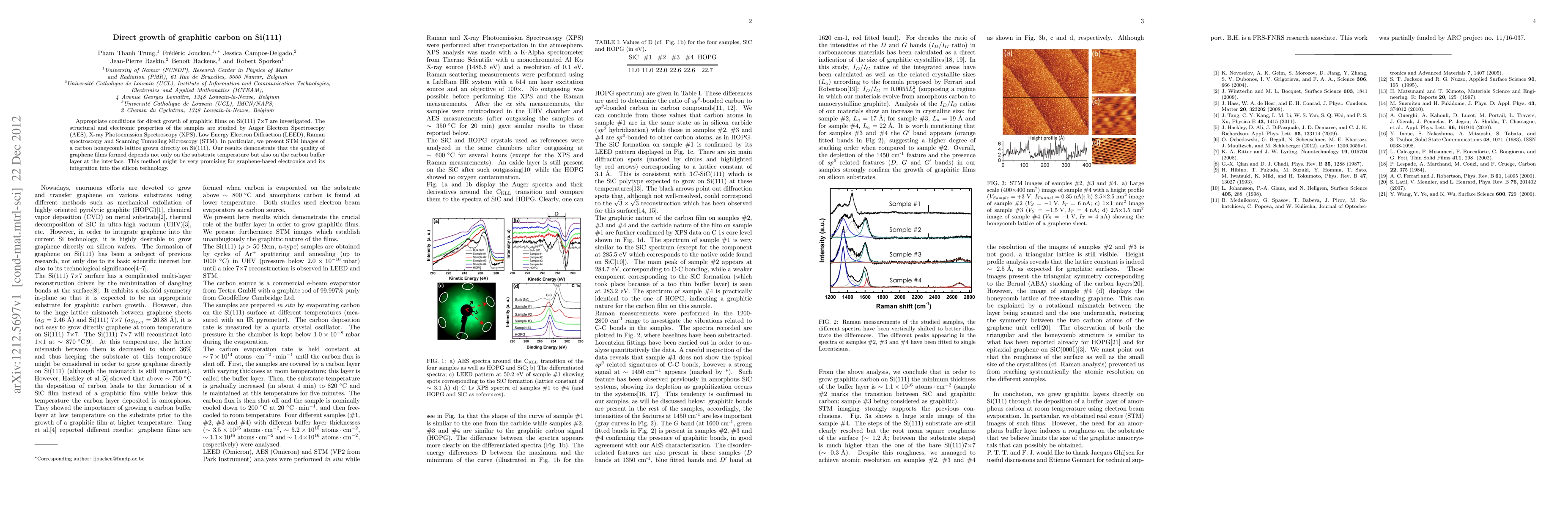
ArxivLens

Quick Summary:

This paper investigates optimal conditions for growing high-quality graphitic films directly on Si(111) substrates, using various spectroscopic and microscopic techniques. The study finds that both substrate temperature and the presence of a carbon buffer layer are crucial for achieving a honeycomb lattice structure, suggesting potential for graphene integration in silicon-based electronics.

DOI: 10.1063/1.4773989
arXiv Id: 1212.5697
Comments: Accepted in APL
Date Published: 2015-06-12
Date Updated: 2015-06-12

Categories:

Key Terms (TF-IDF):

spectroscopy (0.279)
carbon (0.265)
si (0.265)
graphene (0.261)
films (0.257)
electron (0.190)
raman (0.177)
substrate (0.164)
scanning (0.163)
diffraction (0.159)
tunneling (0.159)
silicon (0.158)
microscopy (0.153)
results demonstrate (0.146)
interface (0.142)
formed (0.138)
low energy (0.138)
integration (0.137)
structural (0.136)
technology (0.133)
License: http://arxiv.org/licenses/nonexclusive-distrib/1.0/

Summary:

Appropriate conditions for direct growth of graphitic films on Si(111) 7$\times$7 are investigated. The structural and electronic properties of the samples are studied by Auger Electron Spectroscopy (AES), X-ray Photoemission Spectroscopy (XPS), Low Energy Electron Diffraction (LEED), Raman spectroscopy and Scanning Tunneling Microscopy (STM). In particular, we present STM images of a carbon honeycomb lattice grown directly on Si(111). Our results demonstrate that the quality of graphene films formed depends not only on the substrate temperature but also on the carbon buffer layer at the interface. This method might be very promising for graphene-based electronics and its integration into the silicon technology.

Citation & Reference Network Visualization

This graph shows how this paper is connected to other research. The current paper is shown in dark gray, papers that cite it are in green, and papers it references are in blue. You can:

Current Paper
Papers citing this work (Citations)
Papers cited by this work (References)

• Hover over any node to see the paper title

• Click a node to view that paper's details

• Drag nodes to rearrange the graph

• Use the zoom controls (bottom right) to zoom in/out

Citations and References

Title Authors Year Actions
A perspective of recent advances in PECVD-grown graphene thin films for scientific research and technological applications
Chen-Hsuan Lu, Duxing Hao, Nai-Chang Yeh
2024
View Paper
Annealing coatings of graphene on silicon and application to tribology
Le Hoang Tuan, L. Sang
2023
View Paper
CVD growth of high-quality graphene over Ge (100) by annihilation of thermal pits
T. Diallo, M. Aziziyan, R. Arvinte, R. Arès, S. Fafard, A. Boucherif
2021
View Paper
The Fabrication of Wrinkle‐Free Graphene Patterns on Ge(110) Substrate
Tianbo Wang, Panlin Li, Min Gao, Yalan Wang, Z. Di, Z. Xue, Miao Zhang
2021
View Paper
Epitaxial graphene/Ge interfaces: a minireview.
Y. Dedkov, E. Voloshina
2020
View Paper
Direct large-area growth of graphene on silicon for potential ultra-low-friction applications and silicon-based technologies
Wei-Shiuan Tseng, Yen-Chun Chen, Chen-Chih Hsu, Chen-Hsuan Lu, Chih‐I Wu, N. Yeh
2020
View Paper
Graphitic Carbon/Graphene on Si(111) via Direct Deposition of Solid‐State Carbon Atoms: Growth Mechanism and Film Characterization
T. Pham, R. Sporken
2019
View Paper
Direct growth of graphene-like film microstructure on charge pre-patterned SiO2/Si substrate
M. Knyazev, D. Sedlovets, V. I. Korepanov, O. Trofimov, A. Zotov, A. Svintsov
2019
View Paper
MBE Growth of Graphene
J. Lopes
2019
View Paper
Growth of single-layer graphene on Ge (1 0 0) by chemical vapor deposition
C. D. Mendoza, P. G. Caldas, F. Freire, M.E.H. Maia da Costa
2018
View Paper
The chemistry of CVD graphene
Jan Plutnar, M. Pumera, Zdenek Sofer
2018
View Paper
Direct Growth of Graphene on Silicon by Metal-Free Chemical Vapor Deposition
Lixuan Tai, Daming Zhu, Xing Liu, Tieying Yang, Lei Wang, Rui Wang, Sheng Jiang, Zhenhua Chen, Zhongmin Xu, Xiaolong Li
2017
View Paper
Growth and electronic structure of graphene on semiconducting Ge(110)
Julia Tesch, E. Voloshina, M. Fonin, Y. Dedkov
2017
View Paper
Nanostructured transparent conductive films: Fabrication, characterization and applications
L. He, S. Tjong
2016
View Paper
Graphene and Atom‐Thick 2D Materials: Device Application Prospects
Sungwoo Hwang, J. Heo, Min-Hyun Lee, Kyung‐Eun Byun, Yeonchoo Cho, Seongjun Park
2016
View Paper
The role of SiC as a diffusion barrier in the formation of graphene on Si(111)
T. Pham, C. Santos, F. Joucken, B. Hackens, J. Raskin, R. Sporken
2016
View Paper
From Solid Carbon Sources to Graphene
T. Liang, Yuhan Kong, Hongzheng Chen, Mingsheng Xu
2016
View Paper
Electron-beam assisted selective growth of graphenic carbon thin films on SiO2/Si and quartz substrates
M. Knyazev, D. Sedlovets, O. Trofimov, A. Redkin
2015
View Paper
Graphene base heterojunction transistor: An explorative study on device potential, optimization, and base parasitics
V. D. Lecce, R. Grassi, A. Gnudi, E. Gnani, S. Reggiani, G. Baccarani
2015
View Paper
Carbon out-diffusion mechanism for direct graphene growth on a silicon surface
Byung-Sung Kim, Jong Woon Lee, Yamujin Jang, Soon-Hyung Choi, S. Cha, J. Sohn, Jong Min Kim, Won-Jae Joo, S. Hwang, D. Whang
2015
View Paper
Bottom-up Fabrication of Graphene on Silicon/Silica Substrate via a Facile Soft-hard Template Approach
Yuxing Yang, Ruili Liu, Jiayang Wu, Xinhong Jiang, Pan Cao, Xiaofeng Hu, Ting Pan, Ciyuan Qiu, Junyi Yang, Yinglin Song, Dongqing Wu, Yikai Su
2015
View Paper
Thermoelectric Properties of Nanowires with a Graphitic Shell.
Jong Woon Lee, Eun Kyung Lee, B. Kim, Jae Hyun Lee, H. Kim, Hyeon-Sik Jang, S. Hwang, B. Choi, D. Whang
2015
View Paper
The optimization of a self-focusing e-beam evaporator for carbon evaporation and the application for graphene growth
Shuangming Chen, L. Fan, Jian-Ping Wang, Y. Pan, F. Chen, P. Xu, C. Zou, Zhanghua Wu, Zhanghua Wu
2014
View Paper
Direct growth of graphene on Si(111)
P. T. Trung, J. Campos-Delgado, F. Joucken, J. Colomer, B. Hackens, J. Raskin, C. Santos, S. Robert
2014
View Paper
Wafer-Scale Growth of Single-Crystal Monolayer Graphene on Reusable Hydrogen-Terminated Germanium
Jae‐Hyun Lee, Eun Kyung Lee, Won-Jae Joo, Yamujin Jang, Byung-Sung Kim, Jae‐Young Lim, Soon-Hyung Choi, S. Ahn, J. Ahn, M. Park, Cheol‐Woong Yang, B. Choi, S. Hwang, D. Whang
2014
View Paper
Mesoscopic conductance fluctuations in multi-layer graphene
C. Chuang, Li-Hung Lin, N. Aoki, T. Ouchi, A. Mahjoub, Tak-Pong Woo, R. Puddy, Y. Ochiai, Charles G. Smith, C. Liang
2013
View Paper
Synthesis of graphene and other two-dimensional materials
Norberto Salazar, C. Márquez, F. Gámiz
2021
View Paper
Local electronic properties of epitaxial graphene nanoflakes on metals and semiconductors
Julia Tesch
2018
View Paper
Chemical vapor deposition and physical characterization of gallium, and carbon-related structures on Si (001) and GaP/Si (001) templates for the growth of graphene layers
K. Werner
2015
View Paper
Graphene: from synthesis to the tailoring
J. Colomer, L. Henrard, P. Lambin, J. Pireaux, R. Sporken
2014
View Paper

Comments (0)

This website uses cookies to ensure you get the best experience. Learn more