Direct Growth of Monolayer MoS$_2$ on Nanostructured Silicon Waveguides
Publication
Metrics
AI Quick Summary
This paper reports the first direct growth of MoS$_2$ monolayers on nanostructured silicon waveguides using CVD, demonstrating conformal growth over complex geometries and interfaces. This transfer-free method offers a scalable approach for integrating 2D materials into photonic devices, overcoming the limitations of transfer-based techniques.
Paper Preview
Abstract
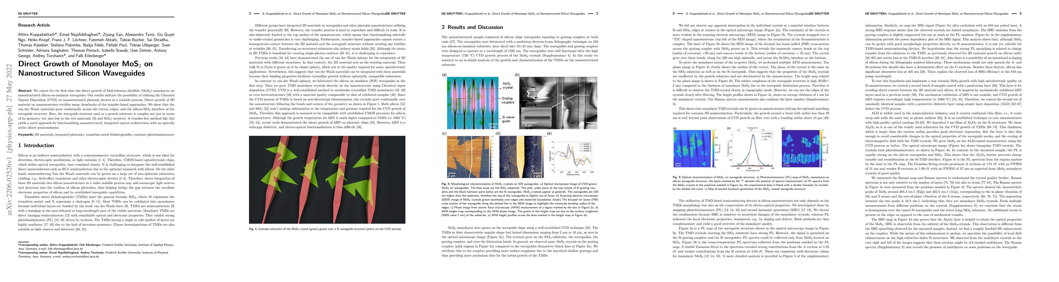
We report for the first time the direct growth of Molybdenum disulfide (MoS$_2$) monolayers on nanostructured silicon-on-insulator waveguides. Our results indicate the possibility of utilizing the Chemical Vapour Deposition (CVD) on nanostructured photonic devices in a scalable process. Direct growth of 2D material on nanostructures rectifies many drawbacks of the transfer-based approaches. We show that the van der Waals materials grow conformally across the curves, edges, and the silicon-SiO$_2$ interface of the waveguide structure. Here, the waveguide structure used as a growth substrate is complex not just in terms of its geometry but also due to the two materials (Si and SiO$_2$) involved. A transfer-free method like this yields a novel approach for functionalizing nanostructured, integrated optical architectures with an optically active direct semiconductor.
AI Key Findings
Get AI-generated insights about this paper's methodology, results, significance, and more — seven facets brought into focus.
Impact
Paper Details
Authors
PDF Preview
Key Terms
Citation Network
Current paper (gray), citations (green), references (blue)
Display is limited for performance on very large graphs.
Discussion 0