Publication
Metrics
Paper Preview
Abstract
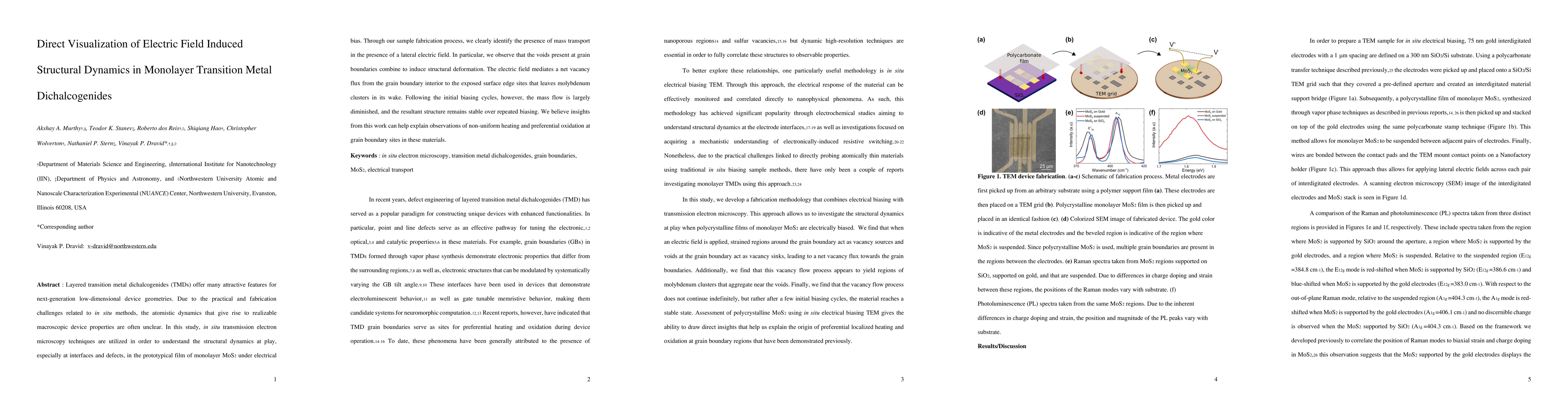
Layered transition metal dichalcogenides (TMDs) offer many attractive features for next-generation low-dimensional device geometries. Due to the practical and fabrication challenges related to in situ methods, the atomistic dynamics that give rise to realizable macroscopic device properties are often unclear. In this study, in situ transmission electron microscopy techniques are utilized in order to understand the structural dynamics at play, especially at interfaces and defects, in the prototypical film of monolayer MoS2 under electrical bias. Through our sample fabrication process, we clearly identify the presence of mass transport in the presence of a lateral electric field. In particular, we observe that the voids present at grain boundaries combine to induce structural deformation. The electric field mediates a net vacancy flux from the grain boundary interior to the exposed surface edge sites that leaves molybdenum clusters in its wake. Following the initial biasing cycles, however, the mass flow is largely diminished, and the resultant structure remains stable over repeated biasing. We believe insights from this work can help explain observations of non-uniform heating and preferential oxidation at grain boundary sites in these materials.
AI Key Findings
Get AI-generated insights about this paper's methodology, results, significance, and more — seven facets brought into focus.
Impact
Paper Details
PDF Preview
Key Terms
Citation Network
Current paper (gray), citations (green), references (blue)
Display is limited for performance on very large graphs.
Discussion 0