Publication
Metrics
AI Quick Summary
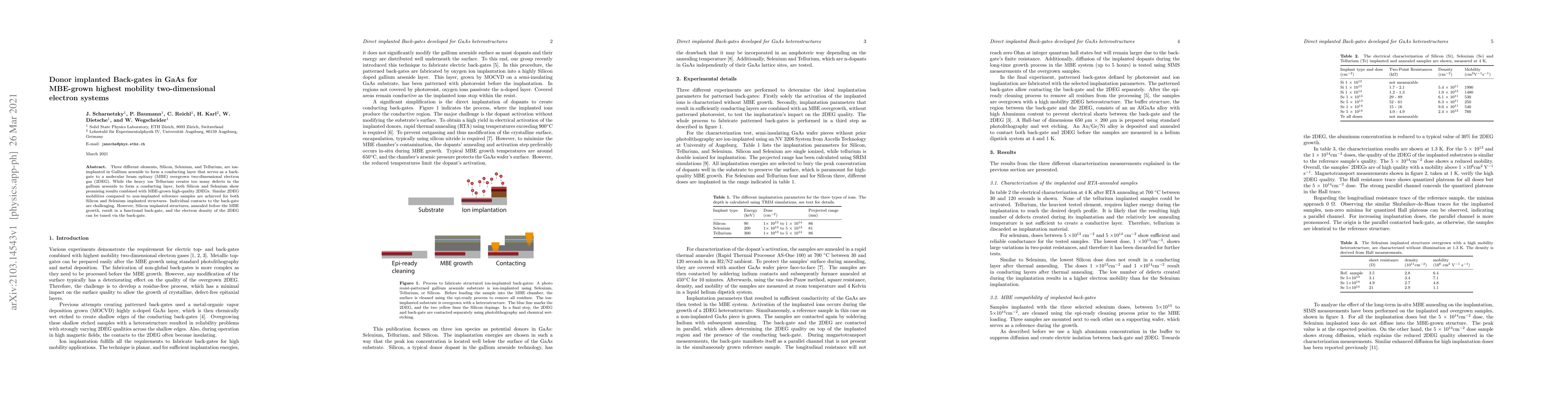
This paper investigates the use of ion-implanted donor elements (Silicon, Selenium, and Tellurium) in Gallium arsenide to create a back-gate for MBE-grown high-mobility two-dimensional electron systems (2DEGs). While Tellurium causes excessive damage, Silicon and Selenium show potential, with Silicon achieving similar 2DEG mobility and tunable electron density when annealed before MBE.
Paper Preview
Abstract
Three different elements, Silicon, Selenium, and Tellurium, are ion-implanted in Gallium arsenide to form a conducting layer that serves as a back-gate to a molecular beam epitaxy (MBE) overgrown two-dimensional electron gas (2DEG). While the heavy ion Tellurium creates too many damages in the gallium arsenide to form a conducting layer, both Silicon and Selenium show promising results combined with MBE-grown high-quality 2DEGs. Similar 2DEG mobility compared to non-implanted reference samples is achieved for both Silicon and Selenium implanted structures. Individual contacts to the back-gate are challenging. However, Silicon implanted structures, annealed before the MBE growth, result in a function back-gate, and the electron density of the 2DEG is tuned via the back-gate.
AI Key Findings
Get AI-generated insights about this paper's methodology, results, significance, and more — seven facets brought into focus.
Impact
Paper Details
Authors
PDF Preview
Key Terms
Citation Network
Current paper (gray), citations (green), references (blue)
Display is limited for performance on very large graphs.
Discussion 0