Double-sided van der Waals epitaxy of topological insulators across an atomically thin membrane
Publication
Metrics
AI Quick Summary
This paper reports the successful double-sided van der Waals epitaxy of topological insulators (Sb$_2$Te$_3$ and Bi$_2$Se$_3$) on atomically thin graphene or hBN membranes, enabling the growth of 2D material heterostructures. It demonstrates the epitaxial tunnel junctions and reveals energy-momentum-spin resonant tunneling of Dirac electrons through field-angle dependent magneto-tunnelling spectroscopy.
Paper Preview
Abstract
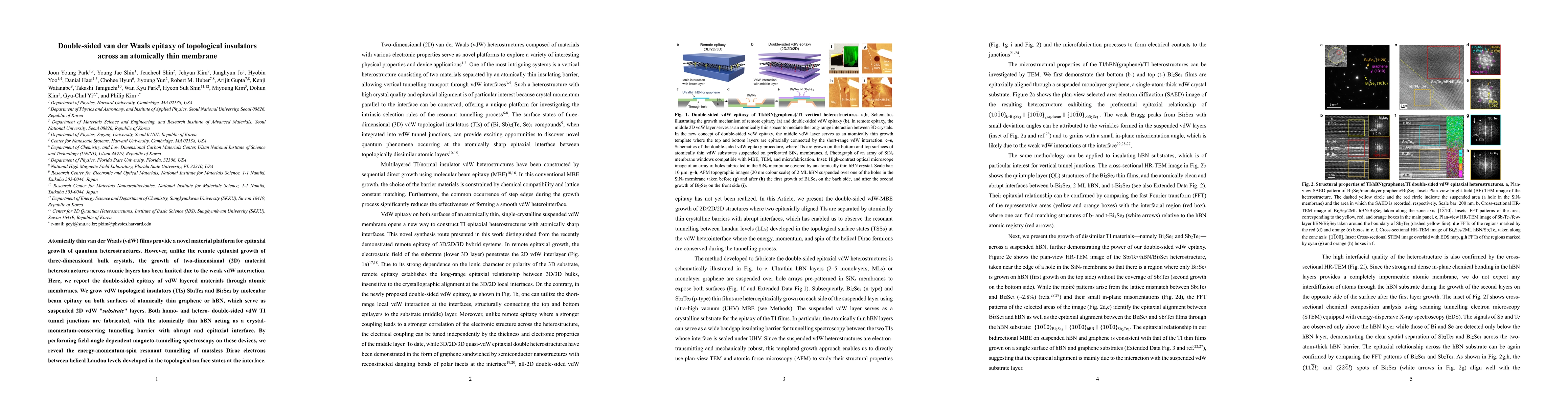
Atomically thin van der Waals (vdW) films provide a novel material platform for epitaxial growth of quantum heterostructures. However, unlike the remote epitaxial growth of three-dimensional bulk crystals, the growth of two-dimensional (2D) material heterostructures across atomic layers has been limited due to the weak vdW interaction. Here, we report the double-sided epitaxy of vdW layered materials through atomic membranes. We grow vdW topological insulators (TIs) Sb$_2$Te$_3$ and Bi$_2$Se$_3$ by molecular beam epitaxy on both surfaces of atomically thin graphene or hBN, which serve as suspended 2D vdW "$\textit{substrate}$" layers. Both homo- and hetero- double-sided vdW TI tunnel junctions are fabricated, with the atomically thin hBN acting as a crystal-momentum-conserving tunnelling barrier with abrupt and epitaxial interface. By performing field-angle dependent magneto-tunnelling spectroscopy on these devices, we reveal the energy-momentum-spin resonant tunnelling of massless Dirac electrons between helical Landau levels developed in the topological surface states at the interface.
AI Key Findings
Get AI-generated insights about this paper's methodology, results, significance, and more — seven facets brought into focus.
Impact
Paper Details
Authors
PDF Preview
Key Terms
Citation Network
Current paper (gray), citations (green), references (blue)
Display is limited for performance on very large graphs.
Discussion 0