Publication
Metrics
AI Quick Summary
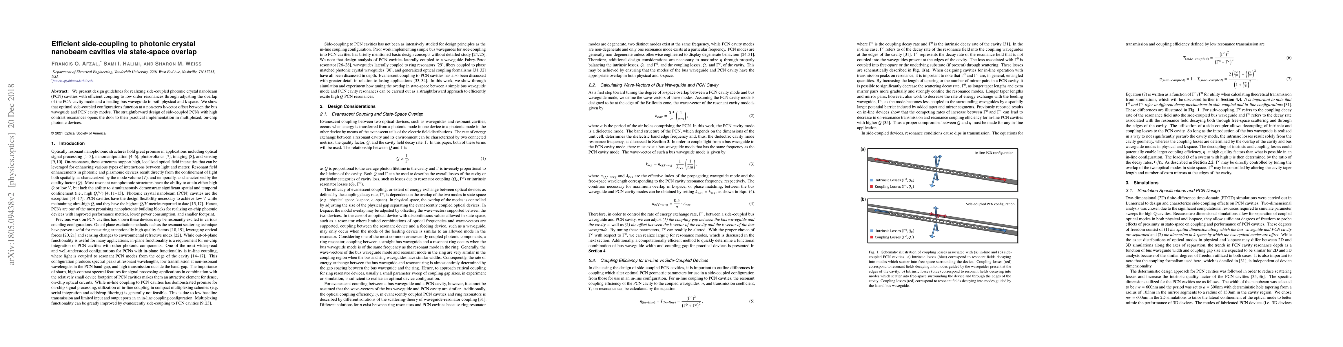
This paper provides design guidelines for efficient side-coupling of photonic crystal nanobeam cavities by optimizing the overlap of cavity modes and feeding waveguides in physical and k-space. It demonstrates that optimal configurations operate with a non-zero k-vector offset, paving the way for practical implementation in multiplexed photonic devices.
Paper Preview
Abstract
We present design guidelines for realizing side-coupled photonic crystal nanobeam (PCN) cavities with efficient coupling to low order resonances through adjusting the overlap of the PCN cavity mode and a feeding bus waveguide in both physical and k-space. We show that optimal side-coupled configurations function at a non-zero k-vector offset between the bus waveguide and PCN cavity modes. The straightforward design of side-coupled PCNs with high contrast resonances opens the door to their practical implementation in multiplexed, on-chip photonic devices.
AI Key Findings
Get AI-generated insights about this paper's methodology, results, significance, and more — seven facets brought into focus.
Impact
Paper Details
PDF Preview
Key Terms
Citation Network
Current paper (gray), citations (green), references (blue)
Display is limited for performance on very large graphs.
Discussion 0