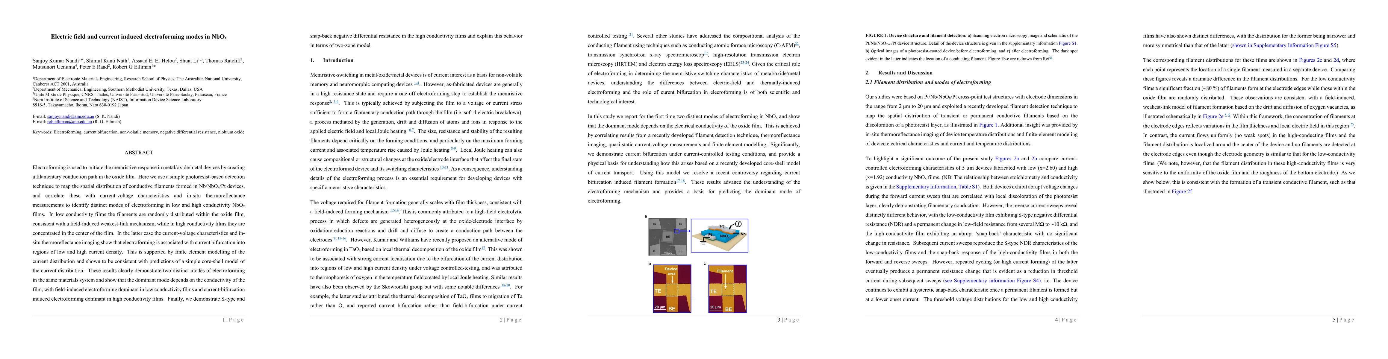
Electric field and current induced electroforming modes in NbOx
Publication
Metrics
AI Quick Summary
This paper investigates two distinct electroforming modes in Nb/NbOx/Pt devices, revealing that low conductivity NbOx films exhibit field-induced electroforming with randomly distributed filaments, while high conductivity films show current bifurcation-induced electroforming concentrated in the center. The study demonstrates S-type and snap-back negative differential resistance in high conductivity films, explained by a two-zone model.
Paper Preview
Abstract
Electroforming is used to initiate the memristive response in metal/oxide/metal devices by creating a filamentary conduction path in the oxide film. Here we use a simple photoresist-based detection technique to map the spatial distribution of conductive filaments formed in Nb/NbOx/Pt devices, and correlate these with current-voltage characteristics and in-situ thermoreflectance measurements to identify distinct modes of electroforming in low and high conductivity NbOx films. In low conductivity films the filaments are randomly distributed within the oxide film, consistent with a field-induced weakest-link mechanism, while in high conductivity films they are concentrated in the center of the film. In the latter case the current-voltage characteristics and in-situ thermoreflectance imaging show that electroforming is associated with current bifurcation into regions of low and high current density. This is supported by finite element modelling of the current distribution and shown to be consistent with predictions of a simple core-shell model of the current distribution. These results clearly demonstrate two distinct modes of electroforming in the same materials system and show that the dominant mode depends on the conductivity of the film, with field-induced electroforming dominant in low conductivity films and current-bifurcation induced electroforming dominant in high conductivity films. Finally, we demonstrate S-type and snap-back negative differential resistance in the high conductivity films and explain this behavior in terms of two-zone model.
AI Key Findings
Get AI-generated insights about this paper's methodology, results, significance, and more — seven facets brought into focus.
Impact
Paper Details
Authors
PDF Preview
Key Terms
Citation Network
Current paper (gray), citations (green), references (blue)
Display is limited for performance on very large graphs.
Discussion 0