Summary

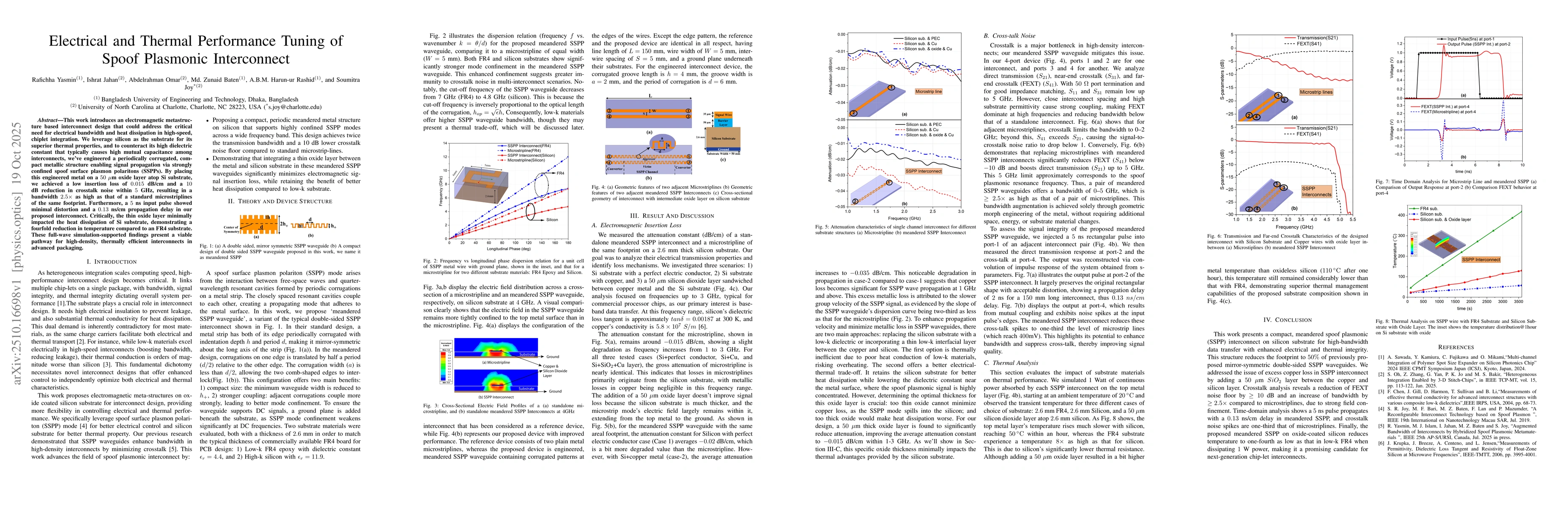
This work introduces an electromagnetic metastructure based interconnect design that could address the critical need for electrical bandwidth and heat dissipation in high-speed, chiplet integration. We leverage silicon as the substrate for its superior thermal properties, and to counteract its high dielectric constant that typically causes high mutual capacitance among interconnects, we've engineered a periodically corrugated, compact metallic structure enabling signal propagation via strongly confined spoof surface plasmon polaritons (SSPPs). By placing this engineered metal on a $50$ $\mu$m oxide layer atop Si substrate, we achieved a low insertion loss of $0.015$ dB/cm and a $10$ dB reduction in crosstalk noise within $5$ GHz, resulting in a bandwidth $2.5\times$ as high as that of a standard microstriplines of the same footprint. Furthermore, a $5$ ns input pulse showed minimal distortion and a $0.13$ ns/cm propagation delay in our proposed interconnect. Critically, the thin oxide layer minimally impacted the heat dissipation of Si substrate, demonstrating a fourfold reduction in temperature compared to an FR4 substrate. These full-wave simulation-supported findings present a viable pathway for high-density, thermally efficient interconnects in advanced packaging.

AI Key Findings

Generated Oct 25, 2025

Methodology

The research employs electromagnetic metastructures on oxide-coated silicon substrates to design interconnects, leveraging spoof surface plasmon polaritons (SSPPs) for signal propagation. Full-wave simulations and experimental validations are used to evaluate electrical and thermal performance.

Key Results

  • Achieved low insertion loss of 0.015 dB/cm and 10 dB reduction in crosstalk noise within 5 GHz
  • Bandwidth 2.5× higher than standard microstrip lines of the same footprint
  • Propagation delay of 0.13 ns/cm with minimal distortion for 5 ns input pulse

Significance

This work addresses critical challenges in high-speed chiplet integration by offering high bandwidth, reduced crosstalk, and improved thermal management, making it suitable for advanced packaging and next-generation interconnects.

Technical Contribution

Development of a meandered SSPP waveguide structure on silicon with a thin oxide layer to enhance electrical performance while maintaining thermal efficiency.

Novelty

Combines periodic corrugated metallic structures with oxide-coated silicon substrates to achieve strong field confinement, enabling high bandwidth and reduced crosstalk in compact interconnects.

Limitations

  • Dependence on full-wave simulations for validation
  • Potential trade-offs in optimizing oxide layer thickness for thermal and electrical performance

Future Work

  • Exploring alternative low-k materials for further thermal optimization
  • Investigating integration with existing PCB fabrication processes

Paper Details

PDF Preview

Download PDF

Comments (0)

This website uses cookies to ensure you get the best experience. Learn more