Electrical excitation of carbon centers in hexagonal boron nitride with tuneable quantum efficiency
Publication
Metrics
AI Quick Summary
This paper reports the successful electrical excitation of carbon centers in hexagonal boron nitride, achieving high quantum efficiency through rational device design. The study utilizes van der Waals technology to control charge dynamics, enabling efficient sub-band-gap electroluminescence and tunable emission energy via Stark effect and band electron screening.
Paper Preview
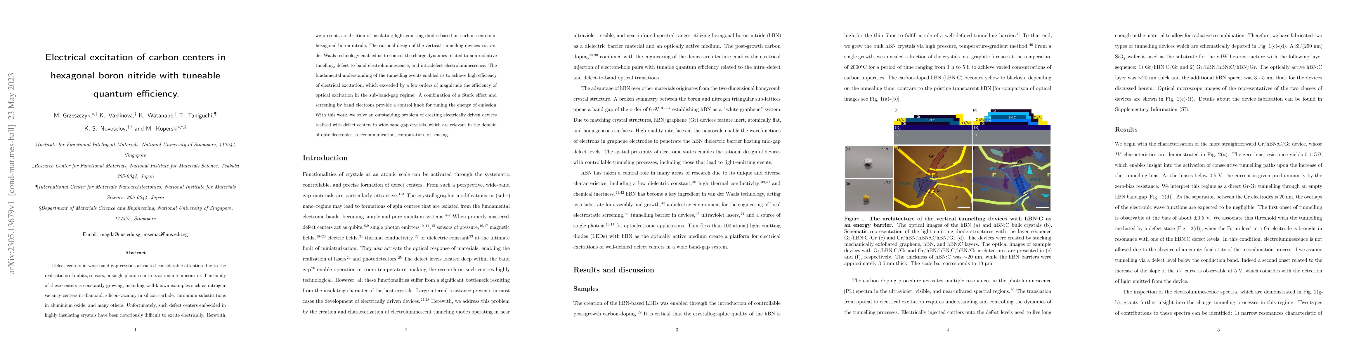
Abstract
Defect centers in wide-band-gap crystals attracted considerable attention due to the realisations of qubits, sensors, or single photon emitters at room temperature. The family of these centers is constantly growing, including well-known examples such as nitrogen-vacancy centers in diamond, silicon-vacancy in silicon carbide, chromium substitutions in aluminium oxide, and many others. Unfortunately, such defect centers embedded in highly insulating crystals have been notoriously difficult to excite electrically. Herewith, we present a realisation of insulating light-emitting diodes based on carbon centers in hexagonal boron nitride. The rational design of the vertical tunnelling devices via van der Waals technology enabled us to control the charge dynamics related to non-radiative tunelling, defect-to-band electroluminescence, and intradefect electroluminescence. The fundamental understanding of the tunnelling events enabled us to achieve high efficiency of electrical excitation, which exceeded by a few orders of magnitude the efficiency of optical excitation in the sub-band-gap regime. A combination of a Stark effect and screening by band electrons provide a control knob for tuning the energy of emission. With this work, we solve an outstanding problem of creating electrically driven devices realised with defect centers in wide-band-gap crystals, which are relevant in the domain of optoelectronics, telecommunication, computation, or sensing.
AI Key Findings
Get AI-generated insights about this paper's methodology, results, significance, and more — seven facets brought into focus.
Impact
Paper Details
Authors
PDF Preview
Key Terms
Citation Network
Current paper (gray), citations (green), references (blue)
Display is limited for performance on very large graphs.
Discussion 0