Publication
Metrics
AI Quick Summary
This paper investigates the electrical switching dynamics and broadband microwave characteristics of vanadium dioxide (VO2) RF devices, demonstrating large resistance modulation and transient switching with two time scales. The study finds an abrupt conductivity jump and oscillatory damping, and shows potential for electromagnetic radiation-induced phase transitions, achieving flat insertion loss and high isolation across frequencies up to 13.5 GHz.
Paper Preview
Abstract
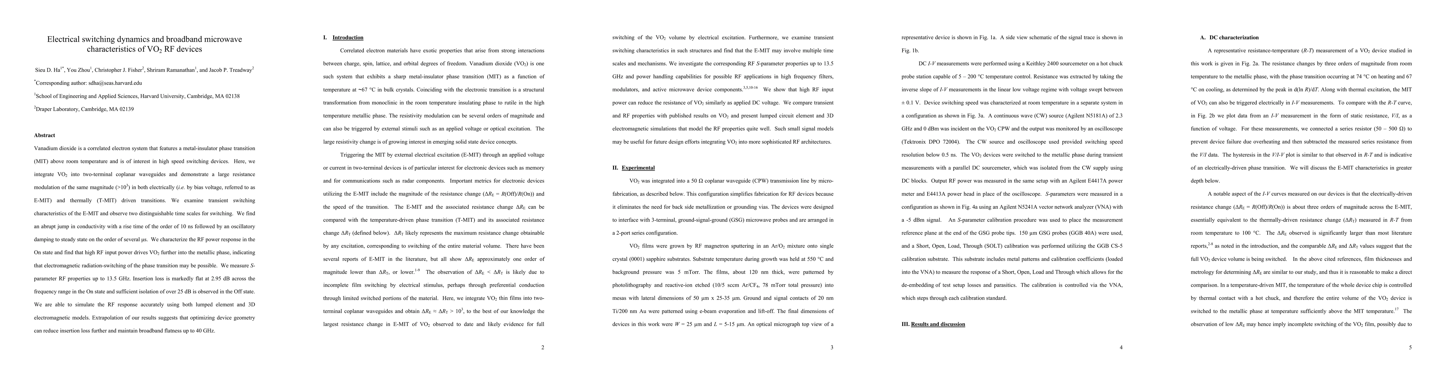
Vanadium dioxide is a correlated electron system that features a metal-insulator phase transition (MIT) above room temperature and is of interest in high speed switching devices. Here, we integrate VO2 into two-terminal coplanar waveguides and demonstrate a large resistance modulation of the same magnitude (>10^3) in both electrically (i.e. by bias voltage, referred to as E-MIT) and thermally (T-MIT) driven transitions. We examine transient switching characteristics of the E-MIT and observe two distinguishable time scales for switching. We find an abrupt jump in conductivity with a rise time of the order of 10 ns followed by an oscillatory damping to steady state on the order of several {\mu}s. We characterize the RF power response in the On state and find that high RF input power drives VO2 further into the metallic phase, indicating that electromagnetic radiation-switching of the phase transition may be possible. We measure S-parameter RF properties up to 13.5 GHz. Insertion loss is markedly flat at 2.95 dB across the frequency range in the On state and sufficient isolation of over 25 dB is observed in the Off state. We are able to simulate the RF response accurately using both lumped element and 3D electromagnetic models. Extrapolation of our results suggests that optimizing device geometry can reduce insertion loss further and maintain broadband flatness up to 40 GHz.
AI Key Findings
Get AI-generated insights about this paper's methodology, results, significance, and more — seven facets brought into focus.
Impact
Paper Details
PDF Preview
Key Terms
Citation Network
Current paper (gray), citations (green), references (blue)
Display is limited for performance on very large graphs.
Discussion 0