01
MethodologyHow they did it
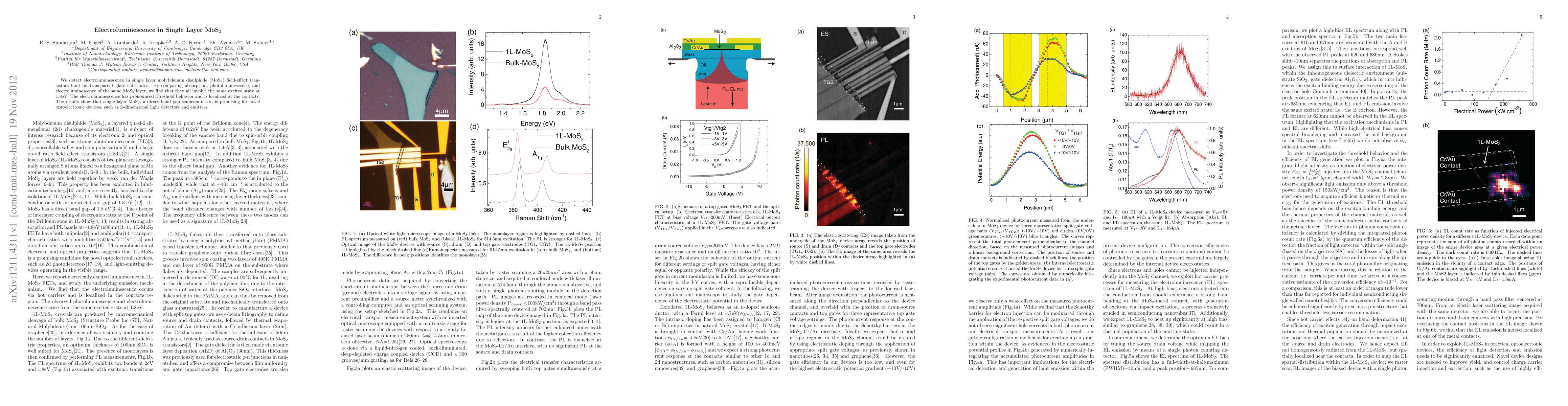
The research utilized single-layer MoS2 field-effect transistors built on transparent glass substrates. Techniques such as Raman spectroscopy, photoluminescence (PL), and electroluminescence (EL) spectroscopy were employed to analyze the optical properties of the MoS2 layer.
Discussion 0