First-principles DFT calculations combined with NEGF quantum transport simulations were performed on bilayer blue phosphorus with a localized bubble deformation to create a geometry‑defined metal–semiconductor–metal homojunction; transmission, tunneling bend resistance, and momentum‑resolved transport were evaluated for varying bubble width and curvature.
Electromechanical Switching and Momentum-Selective Transport in Geometry-Defined Blue Phosphorus Homojunctions
Publication
Metrics
Quick Answers
What methodology did the authors use?
First-principles DFT calculations combined with NEGF quantum transport simulations were performed on bilayer blue phosphorus with a localized bubble deformation to create a geometry‑defined metal–semiconductor–metal homojunction; transmission, tunneling bend resistance, and momentum‑resolved transport were evaluated for varying bubble width and curvature. More in Methodology →
What are the key results?
The bubble‑induced interlayer separation opens a band gap, enabling a clean, chemically‑inert metal–semiconductor–metal homojunction; — Transport switches from ballistic to tunneling, with transmission decaying exponentially with bubble width and only weakly dependent on bubble height; More in Key Results →
Why is this work significant?
This work provides a pathway to fabricate intrinsic, tunable 2D electronic junctions without chemical doping, offering high‑contrast electromechanical switching and precise displacement sensing, and deepens understanding of orbital‑hybridization‑driven transport anisotropy. More in Significance →
What are the main limitations?
The study is purely theoretical; experimental validation of bubble fabrication and transport measurements is pending. — Transport performance depends sensitively on precise bubble geometry and strain, which may be challenging to control reproducibly in practice. More in Limitations →
Abstract
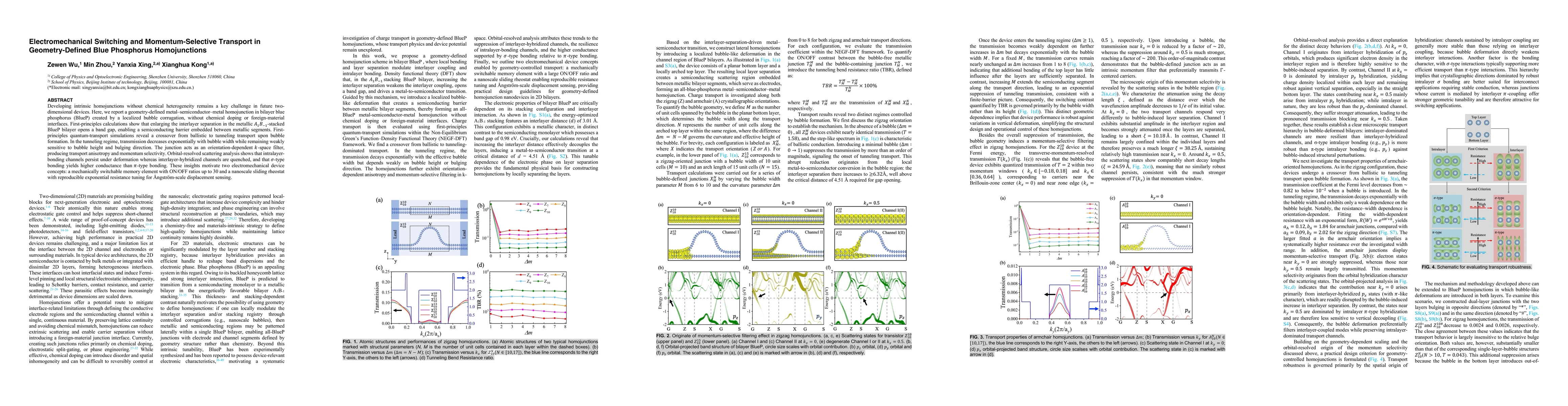
Developing intrinsic homojunctions without chemical heterogeneity remains a key challenge in future two - dimensional devices. Here, we report a geometry - defined metal--semiconductor--metal homojunction in bilayer blue phosphorus (BlueP) created by a localized bubble corrugation, without chemical doping or foreign - material interfaces. First - principles calculations show that enlarging the interlayer separation in the metallic A\(_1\)B\(_1\) - stacked BlueP bilayer opens a band gap, enabling a semiconducting barrier embedded between metallic segments. First - principles quantum - transport simulations reveal a crossover from ballistic to tunneling transport upon bubble formation. In the tunneling regime, transmission decreases exponentially with bubble width while remaining weakly sensitive to bubble height and bulging direction. The junction acts as an orientation - dependent \(k\) - space filter, producing transport anisotropy and momentum selectivity. Orbital - resolved scattering analysis shows that intralayer - bonding channels persist under deformation whereas interlayer - hybridized channels are quenched, and that σ- type bonding yields higher conductance than π- type bonding. These insights motivate two electromechanical device concepts: a mechanically switchable memory element with ON/OFF ratios up to 30 and a nanoscale sliding rheostat with reproducible exponential resistance tuning for Å- scale displacement sensing.
Key Findings, in focus
Seven facets of this paper, analysed and brought into focus by AI.
This work provides a pathway to fabricate intrinsic, tunable 2D electronic junctions without chemical doping, offering high‑contrast electromechanical switching and precise displacement sensing, and deepens understanding of orbital‑hybridization‑driven transport anisotropy.
- The bubble‑induced interlayer separation opens a band gap, enabling a clean, chemically‑inert metal–semiconductor–metal homojunction;
- Transport switches from ballistic to tunneling, with transmission decaying exponentially with bubble width and only weakly dependent on bubble height;
- The junction acts as a momentum‑selective filter—zigzag orientations preferentially transmit Γ‑centered carriers while armchair orientations favor zone‑edge carriers, yielding ON/OFF ratios up to 30 and enabling a nanoscale sliding rheostat for Å‑scale displacement sensing.
This work provides a pathway to fabricate intrinsic, tunable 2D electronic junctions without chemical doping, offering high‑contrast electromechanical switching and precise displacement sensing, and deepens understanding of orbital‑hybridization‑driven transport anisotropy.
The paper establishes a design framework linking interlayer separation, orbital hybridization, and momentum‑selective transport in bilayer blue phosphorus, and demonstrates exponential resistance tuning via lateral sliding of the top layer.
It is the first demonstration of a geometry‑defined, chemically clean metal–semiconductor–metal homojunction in a 2D material, revealing momentum‑selective filtering and proposing a sliding rheostat for nanoscale electromechanical sensing.
- The study is purely theoretical; experimental validation of bubble fabrication and transport measurements is pending.
- Transport performance depends sensitively on precise bubble geometry and strain, which may be challenging to control reproducibly in practice.
- Develop experimental techniques (strain engineering or AFM indentation) to create and characterize bubble‑defined homojunctions and validate the predicted ON/OFF behavior.
- Investigate the influence of external electric, magnetic, or optical fields on orbital hybridization and momentum filtering to enable multifunctional device operation.
Discussion 0