Publication
Metrics
AI Quick Summary
This paper introduces an all-optical electrometer based on optical charge conversion of deep defects in 4H-SiC, demonstrating high-frequency electric field sensing from cryogenic to room temperature with sensitivity of ~41 (V/cm)^2 / √Hz, and also provides spatial 3D maps of surface acoustic wave modes using the piezoelectric character of SiC.
Paper Preview
Abstract
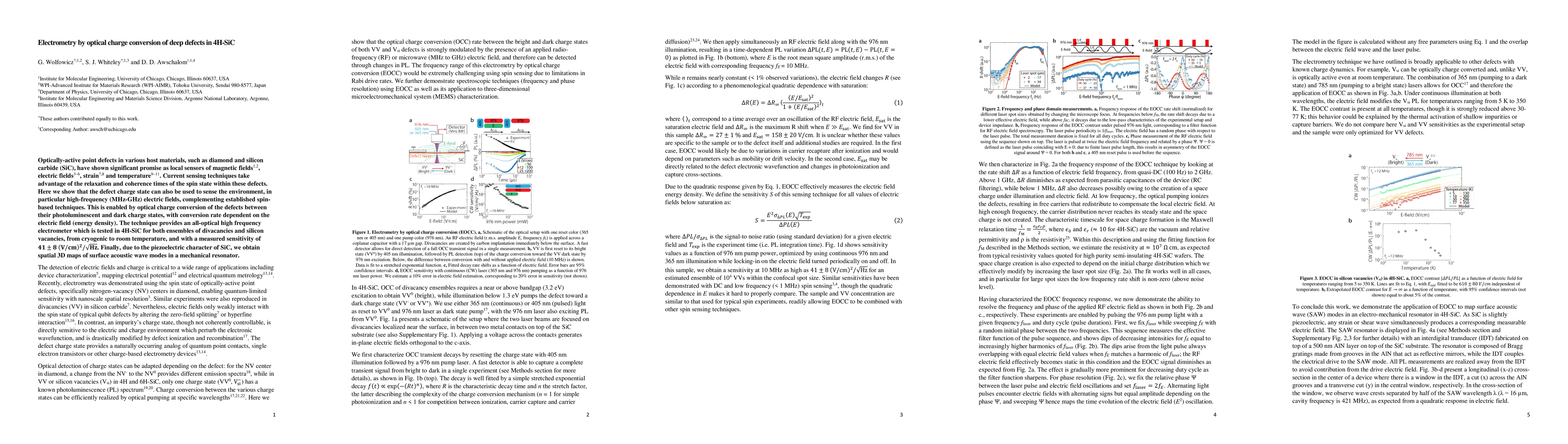
Optically-active point defects in various host materials, such as diamond and silicon carbide (SiC), have shown significant promise as local sensors of magnetic fields, electric fields, strain and temperature. Current sensing techniques take advantage of the relaxation and coherence times of the spin state within these defects. Here we show that the defect charge state can also be used to sense the environment, in particular high frequency (MHz-GHz) electric fields, complementing established spin-based techniques. This is enabled by optical charge conversion of the defects between their photoluminescent and dark charge states, with conversion rate dependent on the electric field (energy density). The technique provides an all-optical high frequency electrometer which is tested in 4H-SiC for both ensembles of divacancies and silicon vacancies, from cryogenic to room temperature, and with a measured sensitivity of ~41 (V/cm)**2 / $\sqrt{Hz}$. Finally, due to the piezoelectric character of SiC, we obtain spatial 3D maps of surface acoustic wave modes in a mechanical resonator.
AI Key Findings
Get AI-generated insights about this paper's methodology, results, significance, and more — seven facets brought into focus.
Impact
Paper Details
PDF Preview
Key Terms
Citation Network
Current paper (gray), citations (green), references (blue)
Display is limited for performance on very large graphs.
Discussion 0