This paper demonstrates the precise manipulation of silicon dopants in graphene using a focused electron beam, achieving greater control than previous methods. It explores the effects of electron energy and implements real-time feedback, paving the way for atomic-level engineering and the development of automated manipulation techniques.
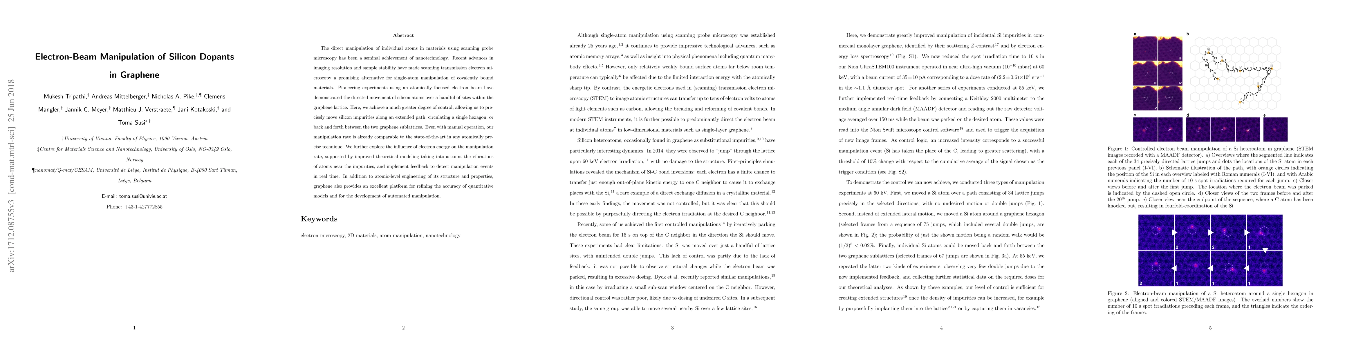
The direct manipulation of individual atoms in materials using scanning probe microscopy has been a seminal achievement of nanotechnology. Recent advances in imaging resolution and sample stability have made scanning transmission electron microscopy a promising alternative for single-atom manipulation of covalently bound materials. Pioneering experiments using an atomically focused electron beam have demonstrated the directed movement of silicon atoms over a handful of sites within the graphene lattice. Here, we achieve a much greater degree of control, allowing us to precisely move silicon impurities along an extended path, circulating a single hexagon, or back and forth between the two graphene sublattices. Even with manual operation, our manipulation rate is already comparable to the state-of-the-art in any atomically precise technique. We further explore the influence of electron energy on the manipulation rate, supported by improved theoretical modeling taking into account the vibrations of atoms near the impurities, and implement feedback to detect manipulation events in real time. In addition to atomic-level engineering of its structure and properties, graphene also provides an excellent platform for refining the accuracy of quantitative models and for the development of automated manipulation.
This graph shows how this paper is connected to other research. The current paper is shown in dark gray, papers that cite it are in green, and papers it references are in blue. You can:
• Hover over any node to see the paper title
• Click a node to view that paper's details
• Drag nodes to rearrange the graph
• Use the zoom controls (bottom right) to zoom in/out
Title | Authors | Year | Actions |
---|---|---|---|
2D isoporous materials: From precursor molecular structures to post-processing methods
|
Yang Yang, Xianhui Li, Cheng Xiang
|
2024
|
View Paper |
Exploring electron-beam induced modifications of materials with machine-learning assisted high temporal resolution electron microscopy
|
M. Boebinger, Ayana Ghosh, Kevin M. Roccapriore, S. Misra, Kai Xiao, Stephen Jesse, M. Ziatdinov, Sergei V. Kalinin, R. Unocic
|
2024
|
View Paper |
Atomic Fabrication of 2D Materials Using Electron Beams Inside an Electron Microscope
|
Mingrui Zhou, Wei Zhang, Jinyi Sun, Fuqiang Chu, Guocai Dong, M. Nie, T. Xu, Litao Sun
|
2024
|
View Paper |
Realizing smart scanning transmission electron microscopy using high performance computing.
|
Utkarsh Pratiush, Austin Houston, Sergei V. Kalinin, Gerd Duscher
|
2024
|
View Paper |
Low-voltage single-atom electron microscopy with carbon-based nanomaterials.
|
Aowen Li, Ang Li, Wu Zhou
|
2024
|
View Paper |
Precision Defect Engineering in 2D Materials via Automated STEM Atomic Fabrication
|
M. Boebinger, Kevin M. Roccapriore, Ayana Ghosh, Kai Xiao, A. Lupini, M. Ziatdinov, Sergei V Kalinin, R. Unocic
|
2024
|
View Paper |
Probing the interaction range of electron beam-induced etching in STEM by a non-contact electron beam
|
S. Noisternig, C. Rentenberger, Christoph Gammer, H. Karnthaler, J. Kotakoski
|
2024
|
View Paper |
Theoretical Understanding of the Structure–Property Relationship of Oxygen-Doped Gallium Selenide as an Efficient Photocatalyst for Oxygen Evolution Reaction
|
Ephrem G. Demissie, C. Siu
|
2024
|
View Paper |
Controlled fabrication of freestanding monolayer SiC by electron irradiation
|
Yunli Da, Ruichun Luo, Bao Lei, Wei Ji, Wu Zhou
|
2024
|
View Paper |
Single atoms and metal nanoclusters anchored to graphene vacancies.
|
A. Trentino, G. Zagler, M. Längle, Jacob Madsen, T. Susi, C. Mangler, E. Åhlgren, K. Mustonen, J. Kotakoski
|
2024
|
View Paper |
Direct Fabrication of Atomically Defined Pores in MXenes Using Feedback-Driven STEM.
|
M. Boebinger, D. Yilmaz, Ayana Ghosh, S. Misra, Tyler S. Mathis, Sergei V. Kalinin, Stephen Jesse, Y. Gogotsi, A. V. van Duin, R. Unocic
|
2024
|
View Paper |
First-Principles Simulation of Beam-Induced Processes Underlying Atomic Manipulation in Electron Microscopes
|
D. Lingerfelt, Panchapakesan Ganesh, J. Jakowski, B. Sumpter
|
2024
|
View Paper |
Disproportionation chemistry in K2PtCl4 visualized at atomic resolution using scanning transmission electron microscopy
|
Jacob G. Smith, Kaustubh J Sawant, Z. Zeng, Tim B. Eldred, Jianbo Wu, Jeffrey P Greeley, Wenpei Gao
|
2024
|
View Paper |
Electronic and magnetic properties of transition-metal-doped monolayer B2S2 within GGA + U framework
|
Wei Chen, Qi Chen, Jianming Zhang, Lin Zhou, Wenxiao Tang, Zhiyou Wang, Jiwei Deng, Shifeng Wang
|
2024
|
View Paper |
The Case for a Defect Genome Initiative
|
Qimin Yan, Swastik Kar, Sugata Chowdhury, A. Bansil
|
2024
|
View Paper |
Characterization of Nanomaterials Using In Situ Liquid-Cell Transmission Electron Microscopy: A Review
|
Yinci Chen, Kuibo Yin, T. Xu, Hongxuan Guo, Litao Sun
|
2023
|
View Paper |
Direct Fabrication of Atomically Defined Pores in MXenes
|
M. Boebinger, D. Yilmaz, Ayana Ghosh, S. Misra, Tyler S. Mathis, Sergei V. Kalinin, S. Jesse, Y. Gogotsi, A. Duin, R. Unocic
|
2023
|
View Paper |
Learning and Controlling Silicon Dopant Transitions in Graphene using Scanning Transmission Electron Microscopy
|
Max Schwarzer, Jesse Farebrother, Joshua Greaves, E. D. Cubuk, Rishabh Agarwal, Aaron C. Courville, Marc G. Bellemare, Sergei V. Kalinin, Igor Mordatch, Pablo Samuel Castro, Kevin M. Roccapriore
|
2023
|
View Paper |
When the atoms dance: exploring mechanisms of electron-beam induced modifications of materials with machine-learning assisted high temporal resolution electron microscopy
|
M. Boebinger, Ayana Ghosh, Kevin M. Roccapriore, S. Misra, Kai Xiao, S. Jesse, M. Ziatdinov, S. Kalinin, R. Unocic
|
2023
|
View Paper |
Probing individual single atom electrocatalyst sites by advanced analytical scanning transmission electron microscopy
|
M. Zachman, Alexey Serov, Xiang Lyu, Samuel Mckinney, Haoran Yu, Mark P. Oxley, Liam Spillane, Edward F. Holby, David A. Cullen
|
2023
|
View Paper |
Orbital Understanding to the Origin of Site-Specific Band Gap Tuning in Electron-Rich S-Doped and Electron Precise C,S-Dual-Doped Graphitic Carbon Nitride
|
M. Sadik N. K, Gibu George, Susmita De
|
2023
|
View Paper |
Challenges for Scaling Up Electron-Beam Manipulation of Graphene Impurities.
|
A. Postl, Eugen Kozyrau, Jacob Madsen, T. Susi
|
2023
|
View Paper |
Fabrication of Atomic-scale Defect Structures within 2D Materials through Automated Electron Beam Control.
|
M. Boebinger, Kevin M. Roccapriore, Ayana Ghosh, Kai Xiao, A. Lupini, M. Ziatdinov, S. Kalinin, R. Unocic
|
2023
|
View Paper |
Opportunities and challenges for DNA in atomic and close-to-atomic scale manufacturing
|
Zhuang Cai, Bei Yang, Rui Gao, Huajie Liu
|
2023
|
View Paper |
Single-atom doped graphene for hydrogen evolution reactions
|
Huimin Hu, Jin-Ho Choi
|
2023
|
View Paper |
Unsupervised machine learning discovery of structural units and transformation pathways from imaging data
|
S. Kalinin, Ondrej Dyck, Ayana Ghosh, Yongtao Liu, B. Sumpter, M. Ziatdinov
|
2023
|
View Paper |
Probe microscopy is all you need
|
S. Kalinin, R. Vasudevan, Yongtao Liu, Ayana Ghosh, Kevin M. Roccapriore, M. Ziatdinov
|
2023
|
View Paper |
Atomically Precise Detection and Manipulation of Nitrogen-Vacancy Centers in Nanodiamonds
|
B. Hudak, Rhonda M. Stroud
|
2023
|
View Paper |
A Platform for Atomic Fabrication and In Situ Synthesis in a Scanning Transmission Electron Microscope
|
Ondrej Dyck, A. Lupini, S. Jesse
|
2023
|
View Paper |
A Core-Shell MWCNT-Pt Nanowire Electron Source with Anomalously Long-Term Stable Field Emission
|
Wenqi Zhang, Pei-Yin Chao, Donglei Chen, Zhan Yang, Lixin Dong
|
2023
|
View Paper |
Topological Defects Created by Gamma Rays in a Carbon Nanotube Bilayer
|
H. Grushevskaya, Andrey Timoshchenko, Ihor Lipnevich
|
2023
|
View Paper |
Atom-by-Atom Direct Writing.
|
O. Dyck, A. Lupini, S. Jesse
|
2023
|
View Paper |
Top‐Down Fabrication of Atomic Patterns in Twisted Bilayer Graphene
|
Ondrej Dyck, Sinchul Yeom, A. Lupini, J. Swett, D. Hensley, M. Yoon, S. Jesse
|
2023
|
View Paper |
Microscopy is All You Need
|
S. Kalinin, R. Vasudevan, Yongtao Liu, Ayana Ghosh, Kevin M. Roccapriore, M. Ziatdinov
|
2022
|
View Paper |
Gate-Tunable Resonance State and Screening Effects for Proton-Like Atomic Charge in Graphene.
|
Mykola Telychko, K. Noori, Hillol Biswas, Dikshant Dulal, Zhaolong Chen, Pin Lyu, Jing Li, H. Tsai, Hanyan Fang, Z. Qiu, Zhun Wai Yap, Kenji Watanabe, T. Taniguchi, Jing Wu, K. Loh, M. Crommie, A. Rodin, Jiong Lu
|
2022
|
View Paper |
Deep learning for electron and scanning probe microscopy: From materials design to atomic fabrication
|
S. Kalinin, M. Ziatdinov, S. Spurgeon, C. Ophus, E. Stach, T. Susi, Josh Agar, John Randall
|
2022
|
View Paper |
Tailoring magnetism in silicon-doped zigzag graphene edges
|
Andoni Ugartemendia, Aran Garcia−Lekue, Elisa Jimenez−Izal
|
2022
|
View Paper |
Probing Electron Beam Induced Transformations on a Single-Defect Level via Automated Scanning Transmission Electron Microscopy.
|
Kevin M. Roccapriore, M. Boebinger, O. Dyck, Ayana Ghosh, R. Unocic, S. Kalinin, M. Ziatdinov
|
2022
|
View Paper |
Atomic-scale Fabrication of 1D-2D Nano Hetero-structures within 2D Materials through Automated Tracking and Electron Beam Control
|
M. Boebinger, Ayana Ghosh, S. Misra, Kevin M. Roccapriore, Kai Xiao, A. Lupini, P. Ganesh, M. Ziatdinov, S. Kalinin, S. Jesse, R. Unocic
|
2022
|
View Paper |
Structure–Property Relationship of Oxygen-Doped Two-Dimensional Gallium Selenide for Hydrogen Evolution Reaction Revealed from Density Functional Theory
|
Ephrem G. Demissie, W. Tang, C. Siu
|
2022
|
View Paper |
Graphene Lattices with Embedded Transition-Metal Atoms and Tunable Magnetic Anisotropy Energy: Implications for Spintronic Devices
|
Rostislav Langer, K. Mustonen, A. Markevich, M. Otyepka, T. Susi, Piotr Błoński
|
2022
|
View Paper |
Three-dimensional
ab initio
description of vibration-assisted electron knock-on displacements in graphene
|
A. Chiriță, A. Markevich, M. Tripathi, N. A. Pike, M. Verstraete, J. Kotakoski, T. Susi
|
2021
|
View Paper |
Fundamentals of atomic and close-to-atomic scale manufacturing:A review
|
Jian Gao, Xichun Luo, F. Fang, Jining Sun
|
2021
|
View Paper |
Aligned Stacking of Nanopatterned 2D Materials for High-Resolution 3D Device Fabrication.
|
Jonas Haas, Finn Ulrich, C. Hofer, Xiao Wang, K. Braun, Jannik C. Meyer
|
2021
|
View Paper |
Electron-Beam Induced Emergence of Mesoscopic Ordering in Layered MnPS3.
|
Kevin M. Roccapriore, Nan Huang, M. Oxley, Vinit Sharma, T. Taylor, S. Acharya, D. Pashov, M. Katsnelson, D. Mandrus, J. Musfeldt, Sergei V. Kalinin
|
2021
|
View Paper |
Atomic-level defect modulation and characterization methods in 2D materials
|
Odongo Francis Ngome Okello, Dong-Hwan Yang, Y. Chu, Sejung Yang, Si-Young Choi
|
2021
|
View Paper |
Transport properties of B/P doped graphene nanoribbon field-effect transistor
|
Chenkang Rui, Cheng Shao, Jiaxu Liu, Aqing Chen, K. Zhu, Q. Shao
|
2021
|
View Paper |
Controlling hydrocarbon transport and electron beam induced deposition on single layer graphene: Toward atomic scale synthesis in the scanning transmission electron microscope
|
Ondrej Dyck, A. Lupini, P. Rack, J. Fowlkes, S. Jesse
|
2021
|
View Paper |
Towards automating structural discovery in scanning transmission electron microscopy
|
Nicole Creange, O. Dyck, R. Vasudevan, M. Ziatdinov, Sergei V. Kalinin
|
2021
|
View Paper |
van der Waals Epitaxy Growth of Bi2Se3 on a Freestanding Monolayer Graphene Membrane: Implications for Layered Materials and Heterostructures
|
J. Lapano, Ondrej Dyck, A. Lupini, Wonhee Ko, Haoxiang Li, H. Miao, Ho Nyung Lee, An‐Ping Li, M. Brahlek, S. Jesse, R. Moore
|
2021
|
View Paper |
Defect-Dependent Corrugation in Graphene.
|
F. Thiemann, P. Rowe, Andrea Zen, E. A. Müller, A. Michaelides
|
2021
|
View Paper |
Mechanism of Electron-Beam Manipulation of Single-Dopant Atoms in Silicon
|
A. Markevich, B. Hudak, Jacob Madsen, Jiaming Song, P. Snijders, A. Lupini, T. Susi
|
2021
|
View Paper |
Exploring electron beam induced atomic assembly via reinforcement learning in a molecular dynamics environment
|
R. Vasudevan, Ayana Ghosh, M. Ziatdinov, Sergei V. Kalinin
|
2021
|
View Paper |
Plasma Treatment of Ultrathin Layered Semiconductors for Electronic Device Applications
|
Jakub Jadwiszczak, D. Kelly, Junqing Guo, Yangbo Zhou, Hongzhou Zhang
|
2021
|
View Paper |
Exploring order parameters and dynamic processes in disordered systems via variational autoencoders
|
Sergei V. Kalinin, O. Dyck, S. Jesse, M. Ziatdinov
|
2021
|
View Paper |
Van der Waals Epitaxy on Freestanding Monolayer Graphene Membrane by MBE
|
J. Lapano, O. Dyck, A. Lupini, Wonhee Ko, Haoxiang Li, H. Miao, Ho Nyung Lee, An‐Ping Li, M. Brahlek, S. Jesse, R. Moore
|
2021
|
View Paper |
Antiferromagnetic spin ordering in two-dimensional honeycomb lattice of SiP3
|
Souren Adhikary, S. Dutta, Sasmita Mohakud
|
2021
|
View Paper |
Imaging Secondary Electron Emission from a Single Atomic Layer.
|
O. Dyck, J. Swett, A. Lupini, J. Mol, S. Jesse
|
2021
|
View Paper |
Doping of Cr in Graphene Using Electron Beam Manipulation for Functional Defect Engineering
|
O. Dyck, M. Yoon, Lizhi Zhang, A. Lupini, J. Swett, S. Jesse
|
2020
|
View Paper |
Unsupervised Machine Learning Discovery of Chemical Transformation Pathways from Atomically-Resolved Imaging Data.
|
Sergei V. Kalinin, O. Dyck, Ayana Ghosh, B. Sumpter, M. Ziatdinov
|
2020
|
View Paper |
Advances and Trends in Chemically Doped Graphene
|
S. Ullah, Qitao Shi, Junhua Zhou, Xiaoqin Yang, Huy Q. Ta, M. Hasan, N. M. Ahmad, L. Fu, A. Bachmatiuk, M. Rümmeli
|
2020
|
View Paper |
Electron beam triggered single-atom dynamics in two-dimensional materials
|
Xiaoxu Zhao, K. Loh, S. Pennycook
|
2020
|
View Paper |
Ferromagnetism in PtTe2 monolayer introduced by doping 3d transition metal atoms and group VA and VIIB atoms
|
Wei Chen, Jian-min Zhang, Xi-guang Wang, Q. Xia, Yaozhuang Nie, G. Guo
|
2020
|
View Paper |
Single Indium Atoms and Few-Atom Indium Clusters Anchored onto Graphene via Silicon Heteroatoms
|
K. Elibol, C. Mangler, D. O’Regan, K. Mustonen, D. Eder, Jannik C. Meyer, J. Kotakoski, R. Hobbs, T. Susi, B. Bayer
|
2020
|
View Paper |
Atomistic Understanding of Damage and Beam-driven Dynamics in 2D Materials
|
A. Chiriță, A. Markevich, J. Kotakoski, T. Susi
|
2020
|
View Paper |
Super-Graphene: The Role of Temperature on Radiation Resistance
|
O. Dyck, J. Swett, Andrew Lupini and Stephen Jesse
|
2020
|
View Paper |
Uncovering the Mechanism for Electron-beam Manipulation of Dopants in Silicon
|
A. Markevich, B. Hudak, A. Lupini, T. Susi
|
2020
|
View Paper |
Imaging Conductivity in a Single Atomic Layer
|
O. Dyck, J. Swett, A. Lupini, S. Jesse
|
2020
|
View Paper |
Understanding and controlling the covalent functionalisation of graphene.
|
Adam J Clancy, Heather Au, N. Rubio, Gabriel O Coulter, M. Shaffer
|
2020
|
View Paper |
Atomic-Scale Localized Thinning and Reconstruction of Two-Dimensional WS2 Layers through In Situ Transmission Electron Microscopy/Scanning Transmission Electron Microscopy
|
Y. Tseng, Kuo-Lun Tai, Chun-Wei Huang, C. Huang, Wen‐Wei Wu
|
2020
|
View Paper |
Machine learning of chemical transformations in the Si-graphene system from atomically resolved images via variational autoencoder
|
Sergei V. Kalinin, O. Dyck, S. Jesse, M. Ziatdinov
|
2020
|
View Paper |
Two-dimensional
CP3
monolayer and its fluorinated derivative with promising electronic and optical properties: A theoretical study
|
Moumita Kar, Ritabrata Sarkar, Sougata Pal, P. Sarkar
|
2020
|
View Paper |
Electron-beam introduction of heteroatomic Pt–Si structures in graphene
|
O. Dyck, Cheng Zhang, P. Rack, J. Fowlkes, B. Sumpter, A. Lupini, Sergei V. Kalinin, S. Jesse
|
2020
|
View Paper |
Graphene-mediated interaction between hydrogen adsorbates
|
K. Noori, Hillol Biswas, S. Y. Quek, A. Rodin
|
2020
|
View Paper |
Variable voltage electron microscopy: Toward atom-by-atom fabrication in 2D materials.
|
O. Dyck, S. Jesse, N. Delby, Sergei V. Kalinin, A. Lupini
|
2020
|
View Paper |
Imaging an unsupported metal–metal bond in dirhenium molecules at the atomic scale
|
Kecheng Cao, S. Skowron, J. Biskupek, C. Stoppiello, C. Leist, E. Besley, A. Khlobystov, U. Kaiser
|
2020
|
View Paper |
Direct matter disassembly via electron beam control: electron-beam-mediated catalytic etching of graphene by nanoparticles
|
O. Dyck, D. Lingerfelt, Songkil Kim, S. Jesse, Sergei V. Kalinin
|
2019
|
View Paper |
Quantum material topology via defect engineering
|
A. Pham, P. Ganesh
|
2019
|
View Paper |
Spatially Controlled Fabrication and Mechanisms of Atomically Thin Nanowell Patterns in Bilayer WS2 Using in Situ High Temperature Electron Microscopy.
|
Jun Chen, G. Ryu, Qianyang Zhang, Y. Wen, Kuo-Lun Tai, Yang Lu, J. Warner
|
2019
|
View Paper |
Defect Engineering in 2D Materials: Precise Manipulation and Improved Functionalities
|
Jie Jiang, T. Xu, Junpeng Lu, Litao Sun, Zhenhua Ni
|
2019
|
View Paper |
Toward Electrochemical Studies on the Nanometer and Atomic Scales: Progress, Challenges, and Opportunities.
|
Sergei V. Kalinin, O. Dyck, N. Balke, S. Neumayer, Wan-Yu Tsai, R. Vasudevan, D. Lingerfelt, M. Ahmadi, M. Ziatdinov, M. Mcdowell, E. Strelcov
|
2019
|
View Paper |
Distinctive optoelectronic properties of nanostructured
MoS2
bilayers
|
V. Mlinar
|
2019
|
View Paper |
Electron-Beam Manipulation of Lattice Impurities in Graphene and Single-Walled Carbon Nanotubes
|
T. Susi, M. Tripathi, K. Mustonen, A. Markevich, C. Mangler, C. Su, Ju Li, J. Idrobo, Jannik C. Meyer, J. Kotakoski
|
2019
|
View Paper |
Quantifying Elastic and Inelastic Electron Irradiation Damage in Transmission Electron Microscopy of 2D Materials
|
T. Susi, T. Lehnert, U. Kaiser, Jannik C. Meyer, J. Kotakoski
|
2019
|
View Paper |
Automated Real-time Analysis of Atomic-resolution STEM Images
|
Jacob Madsen, A. Postl, T. Susi
|
2019
|
View Paper |
Atom-by-atom fabrication with electron beams
|
O. Dyck, M. Ziatdinov, D. Lingerfelt, R. Unocic, B. Hudak, A. Lupini, S. Jesse, Sergei V. Kalinin
|
2019
|
View Paper |
Atomic‐Scale Spectroscopic Imaging of the Extreme‐UV Optical Response of B‐ and N‐Doped Graphene
|
F. Hage, M. Kapetanakis, J. Idrobo, Q. Ramasse, D. Kepaptsoglou
|
2019
|
View Paper |
Quantifying transmission electron microscopy irradiation effects using two-dimensional materials
|
T. Susi, Jannik C. Meyer, J. Kotakoski
|
2019
|
View Paper |
Quantifying transmission electron microscopy irradiation effects using two-dimensional materials
|
T. Susi, Jannik C. Meyer, J. Kotakoski
|
2019
|
View Paper |
Direct Cation Exchange in Monolayer MoS_{2} via Recombination-Enhanced Migration.
|
Shi-ze Yang, Weiwei Sun, Yu‐yang Zhang, Y. Gong, M. Oxley, A. Lupini, P. Ajayan, M. Chisholm, S. Pantelides, Wu Zhou
|
2019
|
View Paper |
Engineering the magnetic properties of PtSe2 monolayer through transition metal doping
|
Moumita Kar, Ritabrata Sarkar, Sougata Pal, P. Sarkar
|
2019
|
View Paper |
Electron‐Beam Manipulation of Silicon Impurities in Single‐Walled Carbon Nanotubes
|
K. Mustonen, A. Markevich, M. Tripathi, H. Inani, Er‐Xiong Ding, A. Hussain, C. Mangler, E. Kauppinen, J. Kotakoski, T. Susi
|
2019
|
View Paper |
Silicon Substitution in Nanotubes and Graphene via Intermittent Vacancies
|
H. Inani, K. Mustonen, A. Markevich, Er‐Xiong Ding, M. Tripathi, A. Hussain, C. Mangler, E. Kauppinen, T. Susi, J. Kotakoski
|
2019
|
View Paper |
Atomic Mechanisms for the Si Atom Dynamics in Graphene: Chemical Transformations at the Edge and in the Bulk
|
M. Ziatdinov, O. Dyck, S. Jesse, Sergei V. Kalinin
|
2019
|
View Paper |
Engineered electronic states in atomically precise artificial lattices and graphene nanoribbons
|
Linghao Yan, P. Liljeroth
|
2019
|
View Paper |
Primary radiation damage: A review of current understanding and models
|
K. Nordlund, S. Zinkle, A. Sand, F. Granberg, R. Averback, R. Stoller, T. Suzudo, L. Malerba, F. Banhart, W. J. Weber, F. Willaime, S. Dudarev, D. Simeone
|
2018
|
View Paper |
Influence of temperature on the displacement threshold energy in graphene
|
Alexandru Ionut Chirita Mihaila, T. Susi, J. Kotakoski
|
2018
|
View Paper |
The microscope revolution that’s sweeping through materials science
|
R. Courtland
|
2018
|
View Paper |
Manifold learning of four-dimensional scanning transmission electron microscopy
|
Xin Li, Ondrej Dyck, M. Oxley, A. Lupini, Leland McInnes, John Healy, S. Jesse, S. Kalinin
|
2018
|
View Paper |
Direct visualization of the 3D structure of silicon impurities in graphene
|
C. Hofer, V. Skákalová, Mohammad R A Monazam, C. Mangler, J. Kotakoski, T. Susi, Jannik C. Meyer
|
2018
|
View Paper |
Tracking atomic structure evolution during directed electron beam induced Si-atom motion in graphene via deep machine learning
|
Ziatdinov Maxim, S. Jesse, B. Sumpter, Sergei V. Kalinin, O. Dyck
|
2018
|
View Paper |
Building and exploring libraries of atomic defects in graphene: Scanning transmission electron and scanning tunneling microscopy study
|
M. Ziatdinov, O. Dyck, Xin Li, B. Sumpter, S. Jesse, R. Vasudevan, Sergei V. Kalinin
|
2018
|
View Paper |
Engineering single-atom dynamics with electron irradiation
|
C. Su, M. Tripathi, Qing-Bo Yan, Zegao Wang, Zihan Zhang, C. Hofer, Haozhe Wang, L. Basile, G. Su, M. Dong, Jannik C. Meyer, J. Kotakoski, J. Kong, J. Idrobo, T. Susi, Ju Li
|
2018
|
View Paper |
Deep analytics of atomically-resolved images: manifest and latent features
|
M. Ziatdinov, O. Dyck, A. Maksov, B. Hudak, A. Lupini, Jiaming Song, P. Snijders, R. Vasudevan, S. Jesse, Sergei V. Kalinin
|
2018
|
View Paper |
A review of CNTs and graphene reinforced YSZ nanocomposites: Preparation, mechanical and anti-irradiation properties
|
Xiaodong Zhang, Chenkun Sun, H. Ji, Mingqi Yang, Haipeng Zhang, W. Tian, Yiyong Wu, O. Tolochko, You Wang
|
2023
|
View Paper |
Probing potential energy landscapes via electron-beam-induced single atom dynamics
|
O. Dyck, M. Ziatdinov, S. Jesse, F. Bao, A. Nobakht, A. Maksov, B. Sumpter, R. Archibald, K. Law, Sergei V. Kalinin
|
2021
|
View Paper |
Other spectroscopic methods for graphene characterization: X-ray and electron spectroscopies
|
T. Susi
|
2021
|
View Paper |
Transmission electron microscopy characterization of graphene
|
J. Meyer
|
2021
|
View Paper |
Imaging and modifying 2D materials by STEM
|
Xiaoxu Zhao
|
2021
|
View Paper |
Quantifying electron irradiation effects in transmission electron microscopy
|
T. Susi, Jannik C. Meyer, J. Kotakoski
|
2019
|
View Paper |
Primary radiation damage Nordlund , Kai 2018-12-15
|
K. Nordlund, S. Zinkle, A. Sand, F. Granberg, R. Averback, R. Stoller, T. Suzudo, L. Malerba, F. Banhart, W. J. Weber, F. Willaime, S. Dudarev, D. Simeone
|
View Paper | |
Learning Silicon Dopant Transitions in Graphene using Scanning Transmission Electron Microscopy
|
View Paper |
Ondrej Dyck, Andrew R. Lupini, Stephen Jesse, Mina Yoon, Jacob L. Swett, Lizhi Zhang
Published: 2023-07-13
Published: 2019-02-12
Comments (0)