Authors
Summary
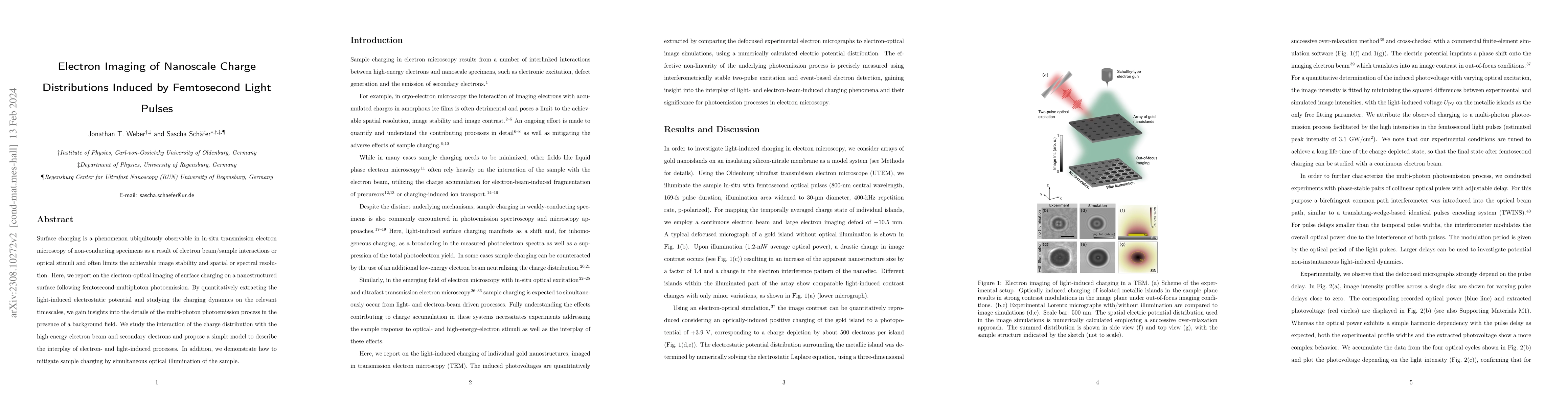
Surface charging is a phenomenon ubiquitously observable in in-situ transmission electron microscopy of non-conducting specimens as a result of electron beam/sample interactions or optical stimuli and often limits the achievable image stability and spatial or spectral resolution. Here, we report on the electron-optical imaging of surface charging on a nanostructured surface following femtosecond-multiphoton photoemission. By quantitatively extracting the light-induced electrostatic potential and studying the charging dynamics on the relevant timescales, we gain insights into the details of the multi-photon photoemission process in the presence of a background field. We study the interaction of the charge distribution with the high-energy electron beam and secondary electrons and propose a simple model to describe the interplay of electron- and light-induced processes. In addition, we demonstrate how to mitigate sample charging by simultaneous optical illumination of the sample.
AI Key Findings
Get AI-generated insights about this paper's methodology, results, and significance.
Paper Details
PDF Preview
Key Terms
Citation Network
Current paper (gray), citations (green), references (blue)
Display is limited for performance on very large graphs.
Similar Papers
Found 4 papersCharge dynamics electron microscopy: nanoscale imaging of femtosecond plasma dynamics
Gabriele Berruto, Eduardo J. C. Dias, F. Javier García de Abajo et al.
Ultrafast Electron Microscopy of Nanoscale Charge Dynamics in Semiconductors
Eduardo J. C. Dias, F. Javier García de Abajo, Ido Kaminer et al.
| Title | Authors | Year | Actions |
|---|
Comments (0)