ArxivLens

Quick Summary:

This study investigates multilayer PdSe$_2$ field-effect transistors under electron irradiation, showing reversible n-type to p-type switching with low electron fluence and irreversible damage at higher fluences, attributed to electron-induced Se vacancy formation and charge trapping at the Si/SiO$_2$ interface.

Journal Reference: Nanotechnology 2020
DOI: 10.1088/1361-6528/ab9472
arXiv Id: 2002.09785
Comments: 15 pages, 4 figures
Date Published: 2020-08-25
Date Updated: 2020-08-25

Key Terms (TF-IDF):

electron (0.224)
device (0.187)
sensitivity (0.178)
vacuum (0.174)
channel (0.161)
type (0.148)
pd (0.144)
induced (0.143)
behavior (0.137)
reached (0.136)
repeated (0.136)
contacts (0.134)
transforms (0.134)
trapping (0.134)
numerical simulation (0.133)
conduction (0.133)
room temperature (0.132)
trap (0.131)
attracted (0.131)
dramatically (0.129)
License: http://arxiv.org/licenses/nonexclusive-distrib/1.0/

Summary:

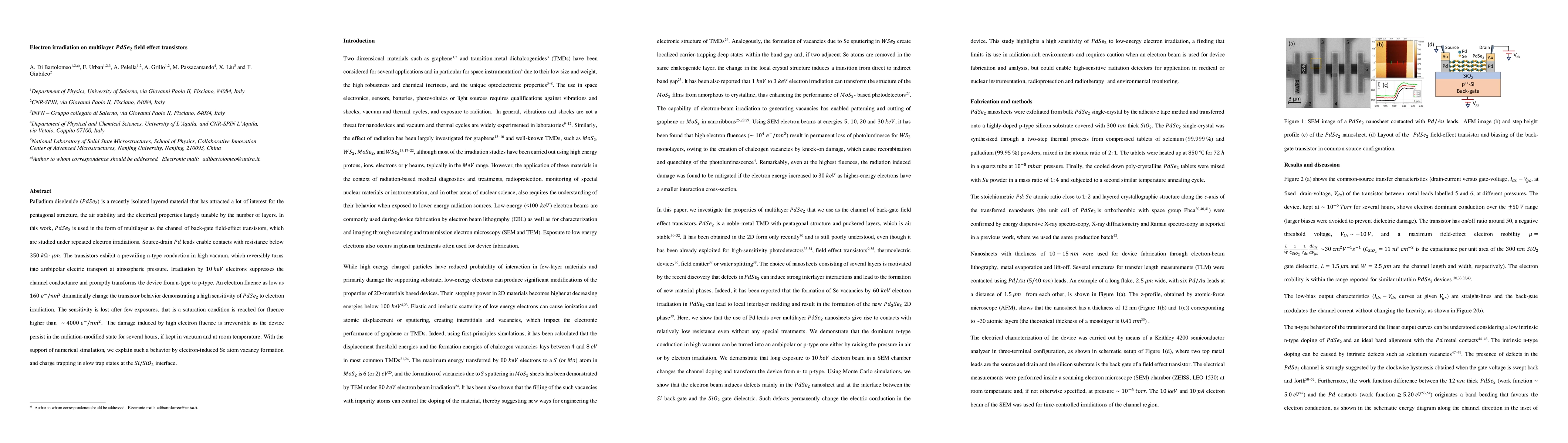
Palladium diselenide (PdSe2) is a recently isolated layered material that has attracted a lot of interest for the pentagonal structure, the air stability and the electrical properties largely tunable by the number of layers. In this work, PdSe2 is used in the form of multilayer as the channel of back-gate field-effect transistors, which are studied under repeated electron irradiations. Source-drain Pd leads enable contacts with resistance below 350 kOhm um. The transistors exhibit a prevailing n-type conduction in high vacuum, which reversibly turns into ambipolar electric transport at atmospheric pressure. Irradiation by 10 keV electrons suppresses the channel conductance and promptly transforms the device from n-type to p-type. An electron fluence as low as 160 e-/nm2 dramatically change the transistor behavior demonstrating a high sensitivity of PdSe2 to electron irradiation. The sensitivity is lost after few exposures, that is a saturation condition is reached for fluence higher than 4000 e-/nm2. The damage induced by high electron fluence is irreversible as the device persist in the radiation-modified state for several hours, if kept in vacuum and at room temperature. With the support of numerical simulation, we explain such a behavior by electron-induced Se atom vacancy formation and charge trapping in slow trap states at the Si/SiO_2 interface.

Citation & Reference Network Visualization

This graph shows how this paper is connected to other research. The current paper is shown in dark gray, papers that cite it are in green, and papers it references are in blue. You can:

Current Paper
Papers citing this work (Citations)
Papers cited by this work (References)

• Hover over any node to see the paper title

• Click a node to view that paper's details

• Drag nodes to rearrange the graph

• Use the zoom controls (bottom right) to zoom in/out

Citations and References

Title Authors Year Actions
Cyclic Atomic Layer Etching of PdSe2
Jieun Kang, Seung Yup Choi, Hye Won Han, Ji Min Kim, Y. Kim, Hyunho Seok, Taesung Kim, D. Kim, Geunyoung Yeom
2024
View Paper
Field enhancement induced by surface defects in two-dimensional ReSe2 field emitters.
F. Giubileo, E. Faella, D. Capista, M. Passacantando, Ofelia Durante, Arun Kumar, A. Pelella, K. Intonti, L. Viscardi, Sebastiano De Stefano, Nadia Martucciello, M. Craciun, S. Russo, A. Di Bartolomeo
2024
View Paper
Influence of Highly Charged Ion Irradiation on the Electrical and Memory Properties of Black Phosphorus Field‐Effect Transistors
S. Sleziona, O. Kharsah, L. Skopinski, Leon Daniel, Jennifer Schmeink, M. Schleberger
2024
View Paper
Electron Irradiation Effect on 2-D WSe2 Phototransistors
Yijing Yang, Shiyu Ling, Pengfei Hou
2024
View Paper
Engineering phonon thermal transport in few-layer PdSe2
Meilin Li, Huanhuan Sun, Jun Zhou, Yunshan Zhao
2023
View Paper
Modulating p-type doping of two dimensional material palladium diselenide
Jiali Yang, Yu Liu, En-Yang Wang, Jinbo Pang, Shirong Huang, T. Gemming, Jinshun Bi, A. Bachmatiuk, Hao Jia, Shu-Xian Hu, Chongyun Jiang, Hong Liu, G. Cuniberti, Weijia Zhou, M. Rümmeli
2023
View Paper
Subthreshold Current Suppression in ReS2 Nanosheet-Based Field-Effect Transistors at High Temperatures
Ofelia Durante, K. Intonti, L. Viscardi, Sebastiano De Stefano, E. Faella, Arun Kumar, A. Pelella, F. Romeo, F. Giubileo, M. S. Alghamdi, M. Alshehri, M. Craciun, S. Russo, A. Di Bartolomeo
2023
View Paper
Temperature-Dependent Conduction and Photoresponse in Few-Layer ReS2
K. Intonti, E. Faella, Arun Kumar, L. Viscardi, F. Giubileo, N. Martucciello, H. T. Lam, K. Anastasiou, M. Craciun, S. Russo, A. Di Bartolomeo
2023
View Paper
Electron Irradiation Engineering Modulated MoS2-Based Phototransistor
Jun Zhang, Zixian Lian, Pengfei Hou
2023
View Paper
Control of Carrier Polarity and Schottky Barriers in Layered PdSe2 Field-Effect Transistors
Miaomiao Li, Wei Luo, Xiangzhe Zhang, Mengjian Zhu, Gang Peng, Z. Zhu, S. Qin
2023
View Paper
Characterization of the electric transport properties of black phosphorous back-gated field-effect transistors
F. Giubileo, A. Pelella, A. Grillo, E. Faella, S. Sleziona, O. Kharsah, M. Schleberger, A. Bartolomeo
2022
View Paper
High-performance broadband photodetector based on PdSe2/black phosphorus heterodiode
Qingsong Dong, Fang Wang, Xin Hu, Yuan Lu, Dong Zhao, Min Zhang, Tao Han, Xing-yuan Hou, Shaoliang Wang, Mingsheng Long, L. Shan
2022
View Paper
Commercial P-Channel Power VDMOSFET as X-ray Dosimeter
G. Ristić, S. Ilić, S. Veljković, Aleksandar S. Jevtić, Strahinja Dimitrijević, A. Palma, S. Stankovic, M. Andjelković
2022
View Paper
Layer-dependent optical and dielectric properties of centimeter-scale PdSe2 films grown by chemical vapor deposition
Mingyang Wei, J. Lian, Yu Zhang, Chenlin Wang, Yueming Wang, Zhen Xu
2022
View Paper
Large In-Plane Anisotropic Terahertz Emission Induced by Asymmetric Polarization in Low-Symmetric PdSe2.
He Wang, Jia-Rong Chang, Yuanyuan Huang, Zhen Lei, Wanyi Du, Yixuan Zhou, Y. E., Xinlong Xu
2021
View Paper
Memory effects in black phosphorus field effect transistors
A. Grillo, A. Pelella, E. Faella, F. Giubileo, S. Sleziona, O. Kharsah, M. Schleberger, A. Di Bartolomeo
2021
View Paper
A progressive journey into 2D-chalcogenide/carbide/nitride-based broadband photodetectors: recent developments and future perspectives
Sukhendu Maity, K. Sarkar, P. Kumar
2021
View Paper
Layer-dependent Optical and Dielectric Properties of Large-size PdSe$_2$ Films Grown by Chemical Vapor Deposition
Mingyang Wei, J. Lian, Yu Zhang, Chenlin Wang, Yueming Wang, Zhen Xu
2021
View Paper
Strain-Driven Switchable Thermal Conductivity in Ferroelastic PdSe2.
Yi Wang, Jie Ren
2021
View Paper
Pentagonal two-dimensional noble-metal dichalcogenide PdSSe for photocatalytic water splitting with pronounced optical absorption and ultrahigh anisotropic carrier mobility
Feng Xiao, Wen Lei, Wei Wang, Lili Xu, Shengli Zhang, Xing Ming
2021
View Paper
Applications of 2D-Layered Palladium Diselenide and Its van der Waals Heterostructures in Electronics and Optoelectronics
Yanhao Wang, Jinbo Pang, Qilin Cheng, Lin Han, Yufen Li, Xue Meng, B. Ibarlucea, Hongbin Zhao, Feng Yang, Haiyun Liu, Hong Liu, Weijia Zhou, Xiao Wang, M. Rummeli, Yu Zhang, G. Cuniberti
2021
View Paper
Electron Irradiation Effect on Van Der Waals Transistor for High-Detectivity Near-Infrared Photodetectors
H. Pengfei, Zhang Yiming, Wang Xinhao, Cai Chuanyang, Guo Hongxia, Zhong Xiangli, Wang Jinbin, Ouyang Xiaoping
2021
View Paper
Electrical Conduction and Photoconduction in PtSe2 Ultrathin Films
A. Di Bartolomeo, F. Urban, E. Faella, A. Grillo, A. Pelella, F. Giubileo, N. McEvoy, F. Gity, P. Hurley
2020
View Paper
Molybdenum Disulfide Field Effect Transistors under Electron Beam Irradiation and External Electric Fields
A. Pelella, A. Grillo, E. Faella, F. Giubileo, F. Urban, A. Bartolomeo
2020
View Paper
Air Pressure, Gas Exposure and Electron Beam Irradiation of 2D Transition Metal Dichalcogenides
A. Di Bartolomeo, A. Pelella, A. Grillo, F. Urban, F. Giubileo
2020
View Paper
Field emission from two-dimensional GeAs
A. Di Bartolomeo, A. Grillo, F. Giubileo, L. Camilli, Jianbo Sun, D. Capista, M. Passacantando
2020
View Paper
Isotropic conduction and negative photoconduction in ultrathin PtSe2 films
F. Urban, F. Gity, P. Hurley, N. McEvoy, A. Di Bartolomeo
2020
View Paper
Electrical transport in two-dimensional PdSe2 and Mos2 nanosheets
A. Di Bartolomeo, F. Urban, A. Pelella, A. Grillo, L. Iemmo, E. Faella, F. Giubileo
2020
View Paper
Electron Irradiation of Metal Contacts in Monolayer MoS2 Field-Effect Transistors
A. Pelella, O. Kharsah, A. Grillo, F. Urban, M. Passacantando, F. Giubileo, L. Iemmo, S. Sleziona, Erik Pollmann, L. Madauß, M. Schleberger, A. Di Bartolomeo
2020
View Paper
Emerging 2D Materials and Their Van Der Waals Heterostructures
A. Di Bartolomeo
2020
View Paper
PtSe2 phototransistors with negative photoconductivity
A. Di Bartolomeo, F. Urban, E. Faella, A. Grillo, A. Pelella, F. Giubileo, M. Askari, N. McEvoy, F. Gity, P. Hurley
2021
View Paper

Comments (0)

This website uses cookies to ensure you get the best experience. Learn more