Publication
Metrics
AI Quick Summary
This paper investigates the potential and charge distribution at the interface between a plasma and a dielectric wall, using a quasi-stationary electron surface layer model. It finds distinct behaviors based on the electron affinity of the dielectric, with different surface charge formations and electron penetration effects.
Paper Preview
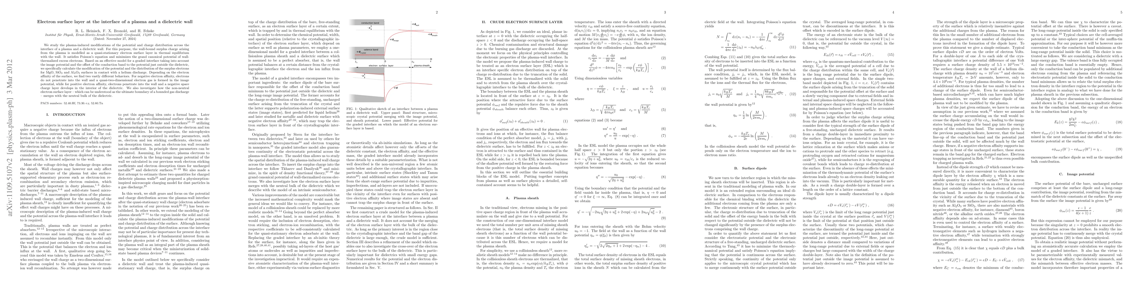
Abstract
We study the potential and the charge distribution across the interface of a plasma and a dielectric wall. For this purpose, the charge bound to the wall is modelled as a quasi-stationary electron surface layer which satisfies Poisson's equation and minimizes the grand canonical potential of the wall-thermalized excess electrons constituting the wall charge. Based on an effective model for a graded interface taking into account the image potential and the offset of the conduction band to the potential just outside the dielectric, we specifically calculate the potential and the electron distribution for magnesium oxide, silicon dioxide and sapphire surfaces in contact with a helium discharge. Depending on the electron affinity of the surface, we find two vastly different behaviors. For negative electron affinity, electrons do not penetrate into the wall and an external surface charge is formed in the image potential, while for positive electron affinity, electrons penetrate into the wall and a space charge layer develops in the interior of the dielectric. We also investigate how the electron surface layer merges with the bulk of the dielectric.
AI Key Findings
Get AI-generated insights about this paper's methodology, results, significance, and more — seven facets brought into focus.
Impact
Paper Details
PDF Preview
Key Terms
Citation Network
Current paper (gray), citations (green), references (blue)
Display is limited for performance on very large graphs.
Discussion 0