Publication
Metrics
AI Quick Summary
This paper demonstrates a method to accurately measure electronic temperatures in metallic nanostructures using the shape of tunnel electroluminescence emission edges in plasmonic nanocavities. It reveals a significant deviation between electronic and lattice temperatures at low temperatures and high currents, attributed to a two-electron process exciting plasmon modes, thus resolving a longstanding controversy on overbias emission in tunnel junctions.
Paper Preview
Abstract
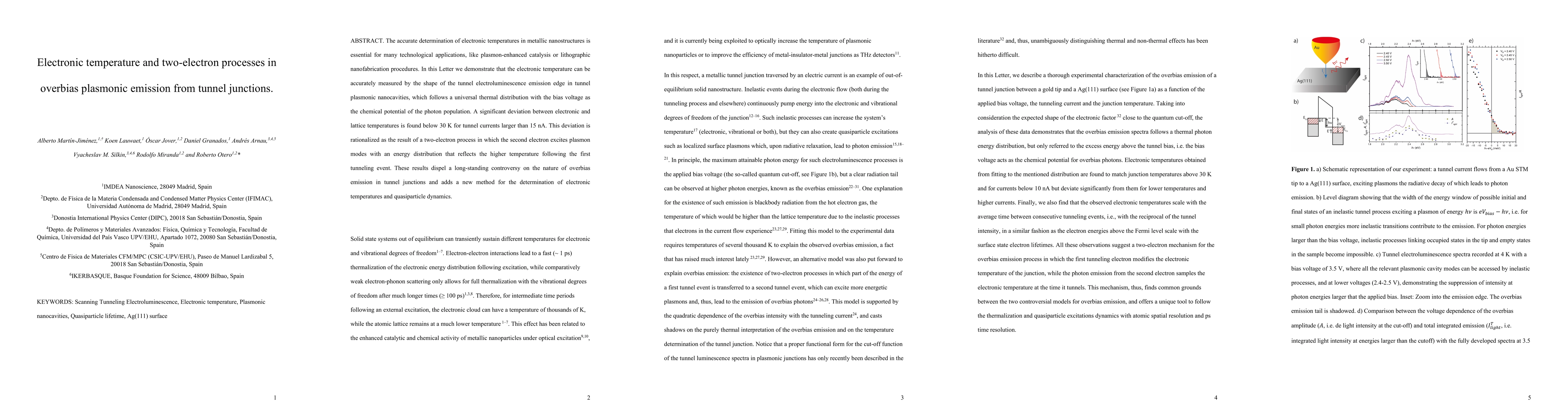
The accurate determination of electronic temperatures in metallic nanostructures is essential for many technological applications, like plasmon-enhanced catalysis or lithographic nanofabrication procedures. In this Letter we demonstrate that the electronic temperature can be accurately measured by the shape of the tunnel electroluminescence emission edge in tunnel plasmonic nanocavities, which follows a universal thermal distribution with the bias voltage as the chemical potential of the photon population. A significant deviation between electronic and lattice temperatures is found below 30 K for tunnel currents larger than 15 nA. This deviation is rationalized as the result of a two-electron process in which the second electron excites plasmon modes with an energy distribution that reflects the higher temperature following the first tunneling event. These results dispel a long-standing controversy on the nature of overbias emission in tunnel junctions and adds a new method for the determination of electronic temperatures and quasiparticle dynamics.
AI Key Findings
Get AI-generated insights about this paper's methodology, results, significance, and more — seven facets brought into focus.
Impact
Paper Details
Authors
PDF Preview
Key Terms
Citation Network
Current paper (gray), citations (green), references (blue)
Display is limited for performance on very large graphs.
Discussion 0