Electronic Trap Detection with Carrier-Resolved Photo-Hall Effect
Publication
Metrics
AI Quick Summary
This paper presents a novel photo-Hall effect method to detect and characterize electronic trap states in semiconductors, revealing trap density and energy levels without altering the material. The technique extracts key carrier properties through a simple hyperbolic relationship, demonstrating its effectiveness on silicon and perovskite photovoltaic films.
Paper Preview
Abstract
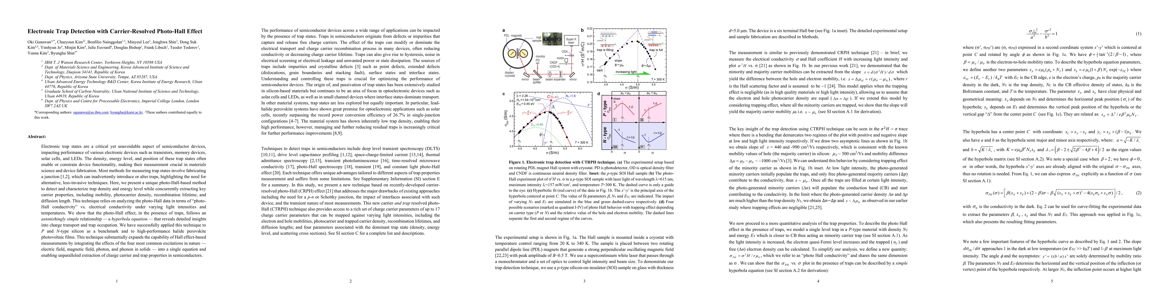
Electronic trap states are a critical yet unavoidable aspect of semiconductor devices, impacting performance of various electronic devices such as transistors, memory devices, solar cells, and LEDs. The density, energy level, and position of these trap states often enable or constrain device functionality, making their measurement crucial in materials science and device fabrication. Most methods for measuring trap states involve fabricating a junction, which can inadvertently introduce or alter traps, highlighting the need for alternative, less-invasive techniques. Here, we present a unique photo-Hall-based method to detect and characterize trap density and energy level while concurrently extracting key carrier properties, including mobility, photocarrier density, recombination lifetime, and diffusion length. This technique relies on analyzing the photo-Hall data in terms of "photo-Hall conductivity" vs. electrical conductivity under varying light intensities and temperatures. We show that the photo-Hall effect, in the presence of traps, follows an $\textit{astonishingly simple}$ relationship - $\textit{a hyperbola equation}$ - that reveals detailed insights into charge transport and trap occupation. We have successfully applied this technique to P and N-type silicon as a benchmark and to high-performance halide perovskite photovoltaic films. This technique substantially expands the capability of Hall effect-based measurements by integrating the effects of the four most common excitations in nature - electric field, magnetic field, photon, and phonon in solids - into a single equation and enabling unparalleled extraction of charge carrier and trap properties in semiconductors.
AI Key Findings
Get AI-generated insights about this paper's methodology, results, significance, and more — seven facets brought into focus.
Impact
Paper Details
Authors
PDF Preview
Citation Network
Current paper (gray), citations (green), references (blue)
Display is limited for performance on very large graphs.
Discussion 0