Publication
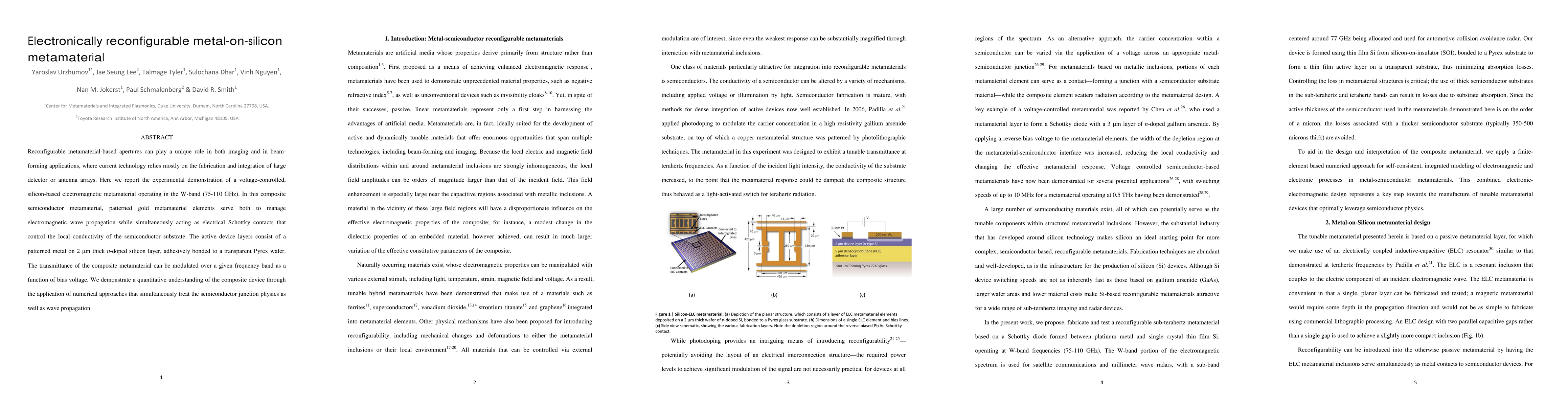
Metrics
AI Quick Summary
This paper presents an electronically reconfigurable metal-on-silicon metamaterial operating in the W-band, where patterned gold elements manage electromagnetic waves and act as electrical contacts to modulate the silicon substrate's conductivity. The device's transmittance can be tuned via bias voltage, validated through numerical simulations.
Paper Preview
Abstract
Reconfigurable metamaterial-based apertures can play a unique role in both imaging and in beam-forming applications, where current technology relies mostly on the fabrication and integration of large detector or antenna arrays. Here, we report the experimental demonstration of a voltage-controlled, silicon-based electromagnetic metamaterial operating in the W-band (75-110 GHz). In this composite semiconductor metamaterial, patterned gold metamaterial elements serve both to manage electromagnetic wave propagation while simultaneously acting as electrical Schottky contacts that control the local conductivity of the semiconductor substrate. The active device layers consist of a patterned metal on a 2-{\mu}m-thick n-doped silicon layer, adhesively bonded to a transparent Pyrex wafer. The transmittance of the composite metamaterial can be modulated over a given frequency band as a function of bias voltage. We demonstrate a quantitative understanding of the composite device through the application of numerical approaches that simultaneously treat the semiconductor junction physics as well as wave propagation.
AI Key Findings
Get AI-generated insights about this paper's methodology, results, significance, and more — seven facets brought into focus.
Impact
Paper Details
PDF Preview
Key Terms
Citation Network
Current paper (gray), citations (green), references (blue)
Display is limited for performance on very large graphs.
Discussion 0