Electrostatic properties and current transport of two-dimensional Schottky barrier diode
Publication
Metrics
AI Quick Summary
This research proposes a new model for understanding carrier distribution and potential profiles in 2D metal-semiconductor heterojunctions, based on first-principle calculations. The model suggests that a stack of 2D graphene-phosphorene Schottky diodes could have a current density ten thousand times higher than a 3D diode, with less energy dissipation.
Paper Preview
Abstract
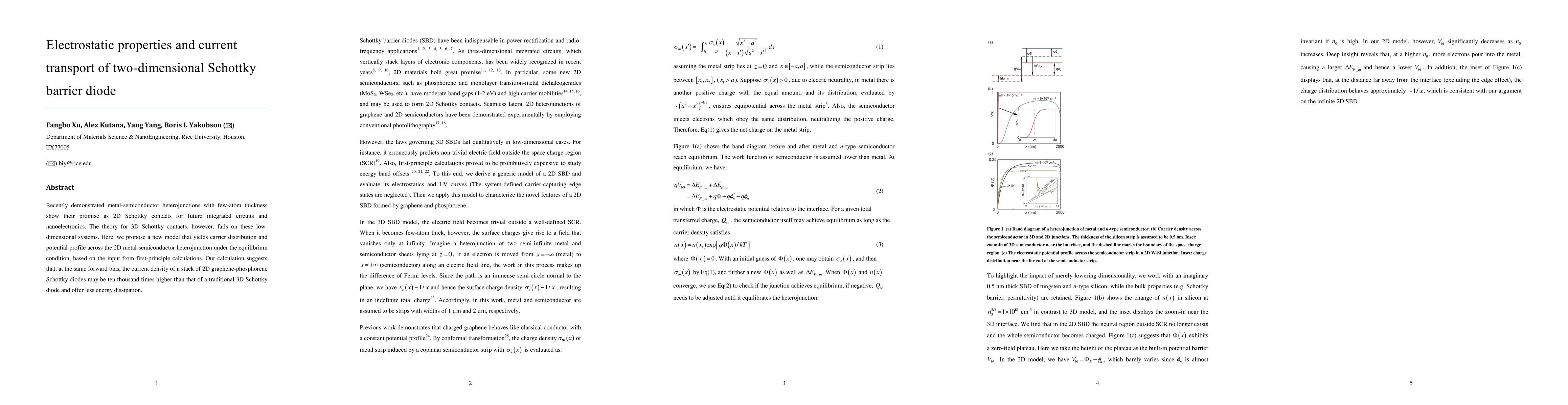
Recently demonstrated metal-semiconductor heterojunctions with few-atom thickness show their promise as 2D Schottky contacts for future integrated circuits and nanoelectronics. The theory for 3D Schottky contacts, however, fails on these low-dimensional systems. Here, we propose a new model that yields carrier distribution and potential profile across the 2D metal-semiconductor heterojunction under the equilibrium condition, based on the input from first-principle calculations. Our calculation also suggests that, at the same forward bias, the current density of a stack of 2D graphene-phosphorene Schottky diodes may be ten thousand times higher than that of a traditional 3D Schottky diode and offer less energy dissipation.
AI Key Findings
Get AI-generated insights about this paper's methodology, results, significance, and more — seven facets brought into focus.
Impact
Paper Details
PDF Preview
Key Terms
Citation Network
Current paper (gray), citations (green), references (blue)
Display is limited for performance on very large graphs.
Discussion 0