This paper investigates the electrostatics of two-dimensional lateral junctions in materials like MoS$_2$ and WSe$_2$, revealing unique properties due to weaker screening compared to bulk materials. The authors develop a conformal mapping technique to accurately solve 2D electrostatic problems, applicable to various junction types and large charge distributions.
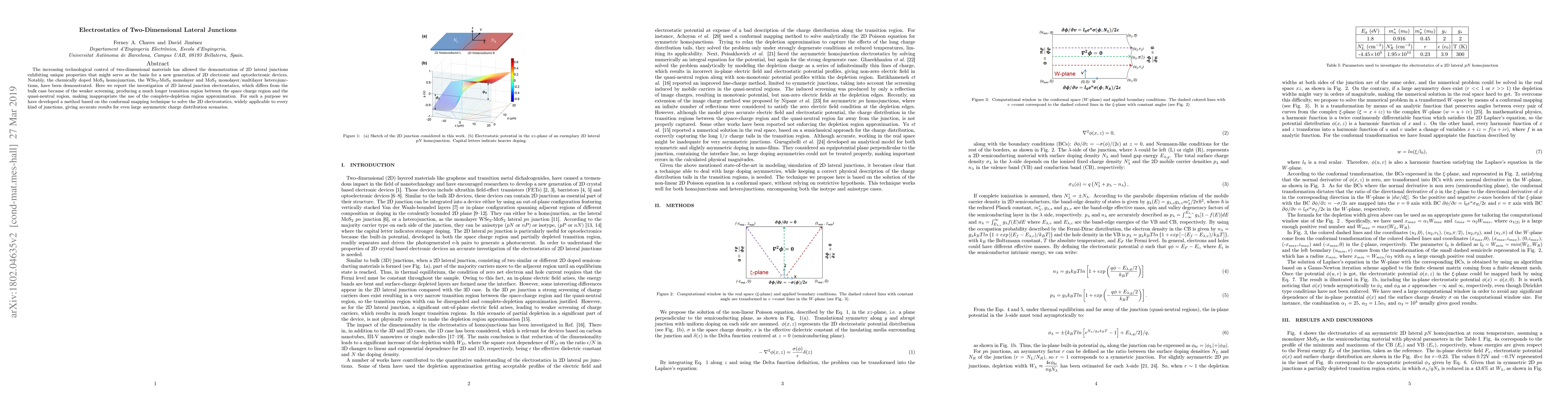
The increasing technological control of two-dimensional materials has allowed the demonstration of 2D lateral junctions, which display unique properties that might serve as the basis for a new generation of 2D electronic and optoelectronic devices. Notably, the chemically doped MoS$_2$ homojunction, the WSe$_2$-MoS$_2$ monolayer and MoS$_2$ monolayer/multilayer heterojunctions, have been demonstrated. Here we report the investigation of 2D lateral junction electrostatics, which differs from the bulk case because of the weaker screening, producing a much longer transition region between the space charge region and the quasi-neutral region, making inappropriate the use of the complete-depletion approximation. For such a purpose we have developed a method based on the conformal mapping technique to solve the 2D electrostatics, which is widely applicable to every kind of junctions, giving accurate results for even large asymmetric charge distribution scenarios.
This graph shows how this paper is connected to other research. The current paper is shown in dark gray, papers that cite it are in green, and papers it references are in blue. You can:
• Hover over any node to see the paper title
• Click a node to view that paper's details
• Drag nodes to rearrange the graph
• Use the zoom controls (bottom right) to zoom in/out
Title | Authors | Year | Actions |
---|---|---|---|
In-Plane Hybrid Structure of h-BN and Graphene for Hydrogen Storage Application: A First-Principles Density Functional Theory Study
|
B. Chettri, P. K. Patra, Yumnam Thakur Singh, Zosiamliana Renthlei, Lalrinkima, Lalrinthara Pachuau, Mohammed Ezzeldien, A. Laref, D. P. Rai
|
2024
|
View Paper |
Additive manufacturing of duplex stainless steels: assessment of deposition processes, microstructure, and properties
|
J. Pacheco, Ana Sofia C. M. de Oliveira
|
2023
|
View Paper |
Structural, magnetic, and optical study of La^3+–Co^2+-substituted Ni_2Y-type barium hexaferrites
|
Shaweta Sharma, T. T. Carol, D. Basandrai, Amit Kumar Srivastava
|
2023
|
View Paper |
Polyvinylidene fluoride—An advanced smart polymer for electromagnetic interference shielding applications—A novel review
|
D. Nivedhitha, S. Jeyanthi
|
2023
|
View Paper |
Gate Tunable Lateral 2D Pn Junctions: An Analytical Study of Its Electrostatics
|
F. Chaves, A. Pacheco-Sánchez, D. Jiménez
|
2023
|
View Paper |
Au decorated ultrathin WS2-based single-electrode triboelectric nanogenerator for flexible self-powered photodetector
|
Tani Chekke, R. Narzary, S. Ngadong, B. Satpati, S. Bayan, U. Das
|
2022
|
View Paper |
Eco-friendly synthesis of cobalt-zinc ferrites using quince extract for adsorption and catalytic applications: An approach towards environmental remediation.
|
T. Tatarchuk, N. Danyliuk, V. Kotsyubynsky, Alena Shumskaya, Egor Kaniukov, Ayman A. Ghfar, M. Naushad, A. Shyichuk
|
2022
|
View Paper |
Structural, Electronic Structure, and Photovoltaic Studies of MgO/TiO2/ITO Heterostructures
|
Deepika Gaur, Sunita Sharma, Aditya Sharma, D. Sharma, S. Shukla
|
2021
|
View Paper |
A New Approach to Designing High-Sensitivity Low-Dimensional Photodetectors.
|
M. Rezaei, S. Bianconi, L. Lauhon, H. Mohseni
|
2021
|
View Paper |
The gate tunable 2D pn junction driven out-of-equilibrium
|
F. Chaves, D. Jiménez
|
2021
|
View Paper |
Homology modeling and molecular docking study of biogenic Muga silk nanoparticles as putative drug‐binding system
|
Prithvi C. Asapur, P. D. Sahare, S. Mahapatra, I. Banerjee
|
2020
|
View Paper |
Interface dark excitons at sharp lateral two-dimensional heterostructures
|
H. Simchi
|
2020
|
View Paper |
2D pn junctions driven out-of-equilibrium
|
F. Chaves, P. C. Feijoo, D. Jim'enez
|
2020
|
View Paper |
Schottky barrier lowering due to interface states in 2D heterophase devices
|
L. Jelver, D. Stradi, K. Stokbro, K. Jacobsen
|
2019
|
View Paper |
Contact-Lifted Thickness-Modulated MoS2 Diodes for Gate-Controlled Electronic Applications
|
Bud Yarrow, A. Askar, A. Parameswaran, M. Adachi
|
2019
|
View Paper |
Pinch-Off Formation in Monolayer and Multilayers MoS2 Field-Effect Transistors
|
Y. Vaknin, R. Dagan, Y. Rosenwaks
|
2019
|
View Paper |
Electrostatics of metal-graphene interfaces: sharp p-n junctions for electron-optical applications.
|
F. Chaves, D. Jiménez, Jaime E. Santos, P. Bøggild, J. Caridad
|
2019
|
View Paper |
Charge transfer across monolayer/bilayer MoS2 lateral interface and its influence on exciton and trion characteristics
|
Hanul Kim, Y. Yoon, Hayoung Ko, S. Kim, H. Rho
|
2019
|
View Paper |
Growth of two-dimensional materials on hexagonal boron nitride (h-BN)
|
Xinsheng Wang, Mongur Hossain, Zhongming Wei, Liming Xie
|
2018
|
View Paper |
Theoretical Estimation of Power Generation Performance of Nano-Sheet Planar Lateral P-N Junction under Illumination
|
Y. Omura
|
2023
|
View Paper |
Anibal Pacheco-Sanchez, Ferney A. Chaves, David Jimenez
Published: 2023-02-07
Comments (0)