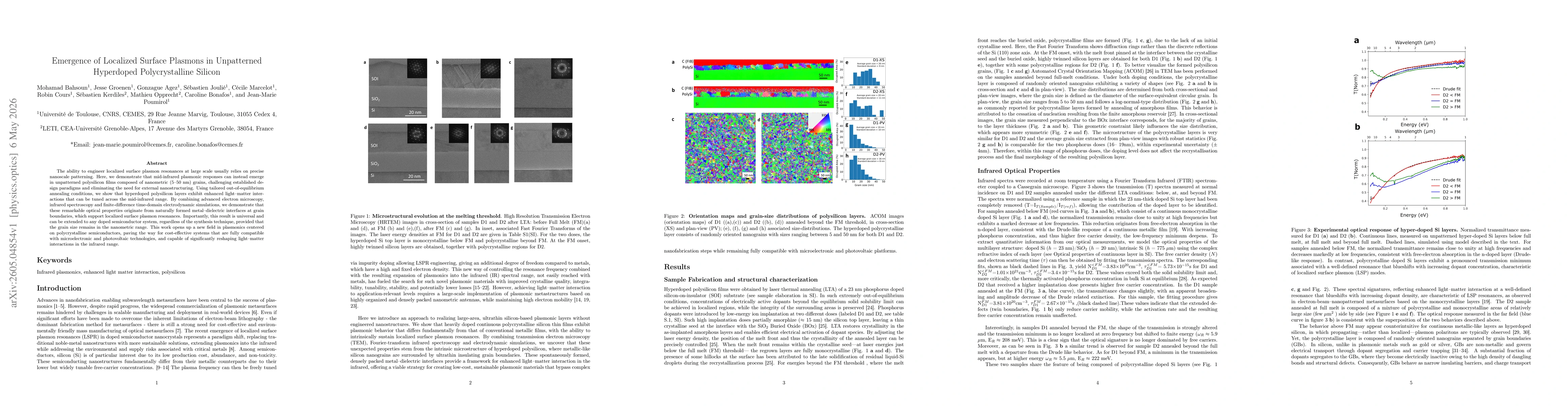
ArxivLens

Publication

Published: May 06, 2026
Categories: physics.optics, cond-mat.mtrl-sci

Metrics

Source: ArXiv

Quick Answers

What methodology did the authors use?

The study combines transmission electron microscopy (TEM), Fourier-transform infrared spectroscopy (FTIR), and finite-difference time-domain (FDTD) electrodynamics simulations to investigate hyperdoped polysilicon films. Structured analysis of grain boundaries reveals intrinsic metal–dielectric interfaces that support localized surface plasmon resonances (LSPRs). The authors compare experimental infrared plasmonic responses with simulations to demonstrate that unpatterned, nanometer-scale grains (5–50 nm) can sustain mid-infrared plasmonics without... More in Methodology →

What are the key results?

Hyperdoped polysilicon films with nanometric grains inherently form metal–dielectric interfaces at grain boundaries, which sustain localized surface plasmon resonances in the mid-infrared range. — Mid-infrared plasmonic responses can be tuned via out-of-equilibrium annealing conditions that modify grain structure and dopant activation, enabling control over light–matter interactions without patterning. More in Key Results →

Why is this work significant?

Demonstrates a universal, pattern-free route to infrared plasmonics in doped semiconductors, potentially reducing manufacturing complexity and enabling integration with microelectronics and photovoltaics. Opens a new field focusing on polycrystalline semiconductors as plasmonic materials, with broad applicability beyond polysilicon. More in Significance →

What are the main limitations?

The study focuses on polysilicon; transferability to other doped semiconductors, while suggested, requires empirical validation across material systems. — Quantitative loss analysis and long-term stability under device operating conditions are not extensively addressed. More in Limitations →

Paper Preview

Abstract

The ability to engineer localized surface plasmon resonances at large scale usually relies on precise nanoscale patterning. Here, we demonstrate that mid-infrared plasmonic responses can instead emerge in unpatterned polysilicon films composed of nanometric (5-50 nm) grains, challenging established design paradigms and eliminating the need for external nanostructuring. Using tailored out-of-equilibrium annealing conditions, we show that hyperdoped polysilicon layers exhibit enhanced light-matter interactions that can be tuned across the mid-infrared range. By combining advanced electron microscopy, infrared spectroscopy and finite-difference time-domain electrodynamic simulations, we demonstrate that these remarkable optical properties originate from naturally formed metal-dielectric interfaces at grain boundaries, which support localized surface plasmon resonances. Importantly, this result is universal and can be extended to any doped semiconductor system, regardless of the synthesis technique, provided that the grain size remains in the nanometric range. This work opens up a new field in plasmonics centered on polycrystalline semiconductors, paving the way for cost-effective systems that are fully compatible with microelectronic and photovoltaic technologies, and capable of significantly reshaping light-matter interactions in the infrared range.

Key Findings, in focus

Seven facets of this paper, analysed and brought into focus by AI.

AI-generated · verify against source Generated May 08, 2026
In focus · one-line synthesis

Demonstrates a universal, pattern-free route to infrared plasmonics in doped semiconductors, potentially reducing manufacturing complexity and enabling integration with microelectronics and photovoltaics.

01
MethodologyHow they did it

The study combines transmission electron microscopy (TEM), Fourier-transform infrared spectroscopy (FTIR), and finite-difference time-domain (FDTD) electrodynamics simulations to investigate hyperdoped polysilicon films. Structured analysis of grain boundaries reveals intrinsic metal–dielectric interfaces that support localized surface plasmon resonances (LSPRs). The authors compare experimental infrared plasmonic responses with simulations to demonstrate that unpatterned, nanometer-scale grains (5–50 nm) can sustain mid-infrared plasmonics without external nanostructuring.

02
ResultsWhat they found
  • Hyperdoped polysilicon films with nanometric grains inherently form metal–dielectric interfaces at grain boundaries, which sustain localized surface plasmon resonances in the mid-infrared range.
  • Mid-infrared plasmonic responses can be tuned via out-of-equilibrium annealing conditions that modify grain structure and dopant activation, enabling control over light–matter interactions without patterning.
  • FTIR measurements and FDTD simulations show strong correspondence, confirming the plasmonic origin of the observed infrared resonances and the role of grain-boundary interfaces.
03
SignificanceWhy it matters

Demonstrates a universal, pattern-free route to infrared plasmonics in doped semiconductors, potentially reducing manufacturing complexity and enabling integration with microelectronics and photovoltaics. Opens a new field focusing on polycrystalline semiconductors as plasmonic materials, with broad applicability beyond polysilicon.

04
Technical ContributionsWhat's new technically

Identification and characterization of naturally formed metal–dielectric interfaces at grain boundaries in hyperdoped polycrystalline silicon as intrinsic plasmonic nano-architectures, enabling mid-infrared LSPRs without external nanostructuring; integration of TEM, FTIR, and FDTD for mechanism elucidation; demonstration of tunable infrared plasmonics solely via annealing- and grain-structure control.

05
NoveltyWhat sets it apart

First demonstration that unpatterned, polycrystalline semiconductor films with nanometer-scale grains can sustain localized surface plasmon resonances in the mid-infrared range through intrinsic grain-boundary interfaces, eliminating the need for nanoscale patterning.

06
LimitationsWhat to be cautious about
  • The study focuses on polysilicon; transferability to other doped semiconductors, while suggested, requires empirical validation across material systems.
  • Quantitative loss analysis and long-term stability under device operating conditions are not extensively addressed.
  • Scalability to large-area uniform grain control and reproducibility across wafers need further demonstration.
07
Future WorkWhere it goes next
  • Extend the approach to other doped semiconductors to validate universality and map plasmonic tunability across material families.
  • Investigate aging and thermal stability of grain-boundary–driven LSPRs under device-relevant operating conditions.
  • Develop processing windows for consistent grain-size distribution at scale to ensure uniform infrared plasmonic responses.

Paper Details

Paper ID: 2605.04854
Comments: 11 pages, 4 figures
Categories:
physics.optics cond-mat.mtrl-sci

How to Cite This Paper

Reference manager: RIS EndNote


Discussion 0

This website uses cookies to ensure you get the best experience. Learn more