This paper introduces an empirical tight-binding method for large-supercell simulations of disordered semiconductor alloys, demonstrating its accuracy in predicting alloy band gaps and providing insights into charge carrier localization and optical transitions in materials like GaAsSb. The method outperforms existing schemes, offering enhanced physical understanding of alloy disorder effects.
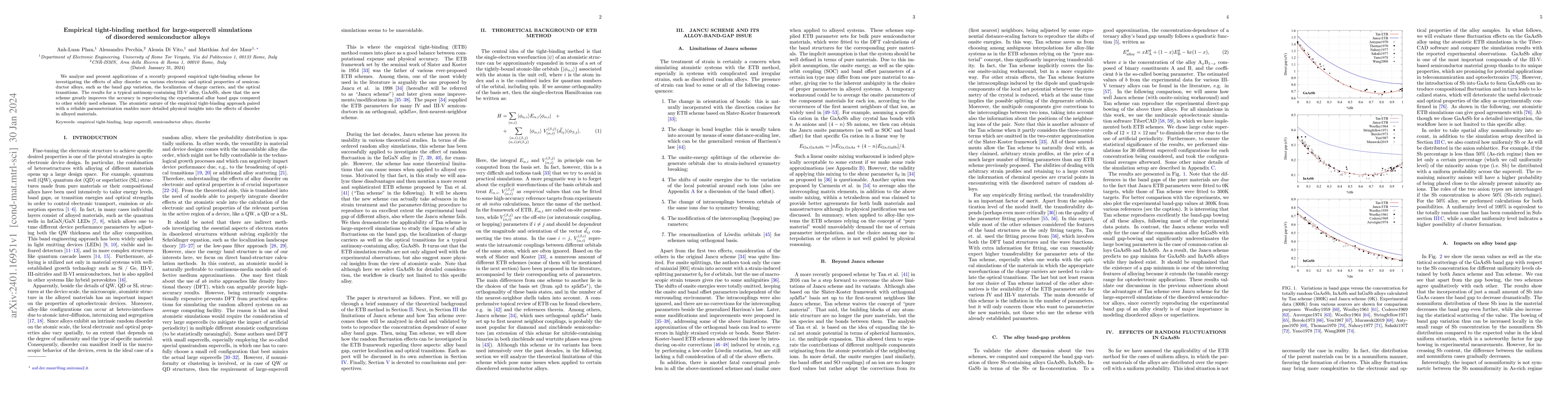
We analyze and present applications of a recently proposed empirical tight-binding scheme for investigating the effects of alloy disorder on various electronic and optical properties of semiconductor alloys, such as the band gap variation, the localization of charge carriers, and the optical transitions. The results for a typical antimony-containing III-V alloy, GaAsSb, show that the new scheme greatly improves the accuracy in reproducing the experimental alloy band gaps compared to other widely used schemes. The atomistic nature of the empirical tight-binding approach paired with a reliable parameterization enables more detailed physical insights into the effects of disorder in alloyed materials.
This graph shows how this paper is connected to other research. The current paper is shown in dark gray, papers that cite it are in green, and papers it references are in blue. You can:
• Hover over any node to see the paper title
• Click a node to view that paper's details
• Drag nodes to rearrange the graph
• Use the zoom controls (bottom right) to zoom in/out
Title | Authors | Year | Actions |
---|---|---|---|
Empirical Tight-Binding Parameterizations for Accurate Heterostructure and Alloy Calculations
|
Anh-Luan Phan, Daniele Soccodato, A. Di Vito, Alessandro Pecchia, M. A. der Maur
|
2024
|
View Paper |
Title | Authors | Year | Actions |
---|---|---|---|
Energy Scales of Compositional Disorder in Alloy Semiconductors
|
S. Baranovskii, A. Nenashev, D. Hertel, F. Gebhard, K. Meerholz
|
2022
|
View Paper |
Quantum states in disordered media. II. Spatial charge carrier distribution
|
A. Nenashev, S. Baranovskii, K. Meerholz, F. Gebhard
|
2022
|
View Paper |
Quantum states in disordered media. I. Low-pass filter approach
|
F. Gebhard, A. Nenashev, K. Meerholz, S. Baranovskii
|
2022
|
View Paper |
Impact of random alloy fluctuations on the electronic and optical properties of (Al,Ga)N quantum wells: Insights from tight-binding calculations.
|
R. Finn, S. Schulz
|
2022
|
View Paper |
Emerging Type‐II Superlattices of InAs/InAsSb and InAs/GaSb for Mid‐Wavelength Infrared Photodetectors
|
D. Alshahrani, M. Kesaria, E. Anyebe, V. Srivastava, D. Huffaker
|
2021
|
View Paper |
Review on GaAsSb nanowire potentials for future 1D heterostructures: Properties and applications
|
Hossein Anabestani, Rassel Shazzad, Fahim Al Fattah, J. Therrien, D. Ban
|
2021
|
View Paper |
Multiscale simulations of the electronic structure of III-nitride quantum wells with varied indium content: Connecting atomistic and continuum-based models
|
D. Chaudhuri, M. O’Donovan, T. Streckenbach, Oliver Marquardt, Patricio Farrell, S. Patra, Thomas Koprucki, Stefan Schulz
|
2021
|
View Paper |
Simulating random alloy effects in III-nitride light emitting diodes
|
A. D. Vito, A. Pecchia, A. D. Carlo, M. Maur
|
2020
|
View Paper |
Bandgap energy determination of InAsSb epilayers grown by molecular beam epitaxy on GaAs substrates
|
Krzysztof Murawski, E. Gomółka, M. Kopytko, K. Grodecki, K. Michalczewski, Ł. Kubiszyn, W. Gawron, P. Martyniuk, A. Rogalski, J. Piotrowski
|
2019
|
View Paper |
On understanding bandgap bowing and optoelectronic quality in Pb–Sn alloy hybrid perovskites
|
A. Rajagopal, R. Stoddard, H. Hillhouse, A. Jen
|
2019
|
View Paper |
GaN surface as the source of non-radiative defects in InGaN/GaN quantum wells
|
C. Haller, J. Carlin, G. Jacopin, W. Liu, Denis Martin, R. Butté, N. Grandjean
|
2018
|
View Paper |
Interplay of morphology, composition, and optical properties of InP-based quantum dots emitting at the 1.55μm telecom wavelength
|
C. Carmesin, M. Schowalter, M. Lorke, D. Mourad, T. Grieb, K. Müller-Caspary, M. Yacob, J. Reithmaier, M. Benyoucef, A. Rosenauer, F. Jahnke
|
2017
|
View Paper |
Impact of Disorder on the Optoelectronic Properties of
GaNyAs1−x−yBix
Alloys and Heterostructures
|
M. Usman, C. Broderick, E. O’Reilly
|
2017
|
View Paper |
Large-scale atomistic simulations demonstrate dominant alloy disorder effects in GaBi x As 1 -x /GaAs multiple quantum wells
|
M. Usman
|
2017
|
View Paper |
Localization landscape theory of disorder in semiconductors. I. Theory and modeling
|
M. Filoche, M. Piccardo, Yuh‐Renn Wu, Chi-kang Li, C. Weisbuch, S. Mayboroda
|
2017
|
View Paper |
Localization landscape theory of disorder in semiconductors. III. Application to carrier transport and recombination in light emitting diodes
|
Chi-kang Li, M. Piccardo, Li-Shuo Lu, S. Mayboroda, L. Martinelli, J. Peretti, J. Speck, C. Weisbuch, M. Filoche, Yuh‐Renn Wu
|
2017
|
View Paper |
Localization landscape theory of disorder in semiconductors. II. Urbach tails of disordered quantum well layers
|
M. Piccardo, Chi-kang Li, Yuh‐Renn Wu, J. Speck, B. Bonef, R. Farrell, M. Filoche, L. Martinelli, J. Peretti, C. Weisbuch
|
2017
|
View Paper |
Atomic intermixing and segregation at the interface of InAs/GaSb type II superlattices
|
Xiaochao Li, Yong Zhang, D. Jiang, F. Guo, Dongbo Wang, Liancheng Zhao
|
2017
|
View Paper |
A review of defects and disorder in multinary tetrahedrally bonded semiconductors
|
L. Baranowski, P. Zawadzki, S. Lany, E. Toberer, A. Zakutayev
|
2016
|
View Paper |
Investigation of Localized States in GaAsSb Epilayers Grown by Molecular Beam Epitaxy
|
Xian Gao, Zhipeng Wei, Fenghuan Zhao, Ya-Hsin Yang, R. Chen, X. Fang, Jilong Tang, D. Fang, Dengkui Wang, Ruixue Li, X. Ge, Xiao-hui Ma, Xiaohua Wang
|
2016
|
View Paper |
Transferable tight-binding model for strained group IV and III-V materials and heterostructures
|
Yaohua Tan, M. Povolotskyi, T. Kubis, T. Boykin, Gerhard Klimeck
|
2016
|
View Paper |
Virtual crystal description of III–V semiconductor alloys in the tight binding approach
|
M. Nestoklon, R. Benchamekh, P. Voisin
|
2016
|
View Paper |
Tight-binding analysis of Si and GaAs ultrathin bodies with subatomic wave-function resolution
|
Yaohua Tan, M. Povolotsky, T. Kubis, T. Boykin, Gerhard Klimeck
|
2015
|
View Paper |
Intrinsic interface states in InAs–AlSb heterostructures
|
F. Raouafi, R. Benchamekh, R. Benchamekh, M. Nestoklon, M. Nestoklon, J. Jancu, P. Voisin
|
2014
|
View Paper |
Advances in mid-infrared detection and imaging: a key issues review
|
M. Razeghi, B. Nguyen
|
2014
|
View Paper |
Controlling radiative loss in quantum well solar cells
|
N. Ekins‐Daukes, K.-H. Lee, L. Hirst, A. Chan, M. Fuhrer, J. Adams, B. Browne, K. Barnham, P. Stavrinou, J. P. Connolly, J. Roberts, B. Stevens, R. Airey, K. Kennedy
|
2013
|
View Paper |
Empirical tight binding parameters for GaAs and MgO with explicit basis through DFT mapping
|
Yaohua Tan, M. Povolotskyi, T. Kubis, Yu He, Zhengping Jiang, Gerhard Klimeck, T. Boykin
|
2012
|
View Paper |
Including strain in atomistic tight-binding Hamiltonians: An application to self-assembled InAs/GaAs and InAs/InP quantum dots
|
M. Zieliński
|
2012
|
View Paper |
Ion beam-mixing effects in nearly lattice-matched AlInN/GaN heterostructures by swift heavy ion irradiation
|
G. Devaraju, S. N. Nageswara Rao, N. Rao, V. Saikiran, T. Chan, T. Osipowicz, M. Breese, A. Pathak
|
2012
|
View Paper |
Strained-Layer Quantum-Well Lasers
|
A. Adams
|
2011
|
View Paper |
Strain-induced, off-diagonal, same-atom parameters in empirical tight-binding theory suitable for [110] uniaxial strain applied to a silicon parametrization
|
T. Boykin, M. Luisier, Mehdi Salmani-Jelodar, Gerhard Klimeck
|
2010
|
View Paper |
Application of Keating's valence force field model to non-ideal wurtzite materials
|
D. Camacho, Y. Niquet
|
2010
|
View Paper |
A SiGe/Si Multiple Quantum Well Avalanche Photodetector
|
P. Sun, Shu-Tong Chang, Yu-Chun Chen, Hongchin Lin
|
2009
|
View Paper |
Quaternary alloy semiconductor nanobelts with bandgap spanning the entire visible spectrum.
|
A. Pan, Ruibin Liu, Minghua Sun, C. Ning
|
2009
|
View Paper |
Onsite matrix elements of the tight-binding Hamiltonian of a strained crystal: Application to silicon, germanium, and their alloys
|
Y. Niquet, D. Rideau, C. Tavernier, H. Jaouen, X. Blase
|
2009
|
View Paper |
TiberCAD: towards multiscale simulation of optoelectronic devices
|
M. Auf der Maur, M. Povolotskyi, F. Sacconi, A. Pecchia, G. Romano, G. Penazzi, A. Di Carlo
|
2008
|
View Paper |
Quantum Dot Solar Cells. Semiconductor Nanocrystals as Light Harvesters
|
P. Kamat
|
2008
|
View Paper |
History, Development, and Applications of High-Brightness Visible Light-Emitting Diodes
|
Russell D. Dupuis, M. Krames
|
2008
|
View Paper |
Characterization of band gap in GaAsSb/GaAs heterojunction and band alignment in GaAsSb/GaAs multiple quantum wells
|
T. S. Wang, J. Tsai, Kuang-I Lin, Jenn-Shyong Hwang, Hao-Hsiung Lin, L. Chou
|
2008
|
View Paper |
TiberCAD: the new multiscale simulator for electronic and optoelectronic devices
|
A. Carlo, F. Sacconi, M. Maur, A. Pecchia, G. Romano, G. Penazzi, M. Povolotskyi
|
2007
|
View Paper |
Tetragonal and trigonal deformations in zinc-blende semiconductors: A tight-binding point of view
|
J. Jancu, P. Voisin
|
2007
|
View Paper |
Approximate bandstructures of semiconductor alloys from tight-binding supercell calculations
|
T. Boykin, N. Kharche, Gerhard Klimeck, M. Korkusiński
|
2007
|
View Paper |
Diagonal parameter shifts due to nearest-neighbor displacements in empirical tight-binding theory
|
T. Boykin, Gerhard Klimeck, R. Bowen, F. Oyafuso
|
2002
|
View Paper |
Tight-binding and k?p models for the electronic structure of Ga(In)NAs and related alloys
|
E. O’Reilly, A. Lindsay, S. Tomić, M. Kamal-Saadi
|
2002
|
View Paper |
Recent progress in quantum cascade lasers and applications
|
C. Gmachl, F. Capasso, D. Sivco, A. Cho
|
2001
|
View Paper |
Band parameters for III–V compound semiconductors and their alloys
|
I. Vurgaftman, J. Meyer, L. Ram-Mohan
|
2001
|
View Paper |
Empirical spds^* tight-binding calculation for cubic semiconductors : general method and material parameters
|
J. Jancu, R. Scholz, F. Beltram, F. Bassani
|
1998
|
View Paper |
Nitride-based semiconductors for blue and green light-emitting devices
|
F. Ponce, D. Bour
|
1997
|
View Paper |
Interface roughness and alloy‐disorder scattering contributions to intersubband transition linewidths
|
K. Campman, H. Schmidt, A. Imamoğlu, A. Gossard
|
1996
|
View Paper |
Electronic density of states of semiconductor alloys from lattice-mismatched isovalent binary constituents.
|
Li, Pötz
|
1992
|
View Paper |
Electronic properties of random alloys: Special quasirandom structures.
|
Su-Huai Wei, L. G. Ferreira, James E. Bernard, A. Zunger
|
1990
|
View Paper |
Special quasirandom structures.
|
A. Zunger, S. Wei, L. G. Ferreira, J. E. Bernard
|
1990
|
View Paper |
Band gaps and spin-orbit splitting of ordered and disordered AlxGa1-xAs and GaAsxSb1-x alloys.
|
Wei, Zunger
|
1989
|
View Paper |
Effect of Disorder on the Conduction-Band Effective Mass, Valence-Band Spin-Orbit Splitting, and the Direct Band Gap in III-V Alloys
|
O. Berolo, J. Woolley, J. A. Vechten
|
1973
|
View Paper |
Liquid Phase Epitaxial Growth of InAs1 − x Sb x
|
G. B. Stringfellow, P. Greene
|
1971
|
View Paper |
Energy gap variation in GaAsxSb1‐x alloys
|
M. Thomas, W. Coderre, J. Woolley
|
1970
|
View Paper |
Liquid Epitaxial Growth of GaAsSb and Its Use as a High‐Efficiency, Long‐Wavelength Threshold Photoemitter
|
G. Antypas, L. W. James
|
1970
|
View Paper |
Conduction bands of GaxIn1–x Sb alloys
|
W. Coderre, J. Woolley
|
1969
|
View Paper |
OPTICAL ENERGY-GAP VARIATION IN InAs–InSb ALLOYS
|
J. Woolley, J. Warner
|
1964
|
View Paper |
Temperature Variation of Optical Energy Gap for GaSb-InSb Alloys
|
J. Woolley, J. Evans
|
1961
|
View Paper |
Optical Energy Gap Variation in the GaSb-InSb System
|
J. Woolley, J. Evans, C. Gillett
|
1959
|
View Paper |
Simplified LCAO Method for the Periodic Potential Problem
|
J. C. Slater, G. Koster
|
1954
|
View Paper |
On the Non‐Orthogonality Problem Connected with the Use of Atomic Wave Functions in the Theory of Molecules and Crystals
|
P. Löwdin
|
1950
|
View Paper |
III-V Ternary and Quaternary Compounds
|
S. Adachi
|
2017
|
View Paper |
Efficiency Drop in Green InGaN = GaN Light Emitting Diodes : The Role of Random Alloy Fluctuations
|
M. Maur, A. Pecchia, G. Penazzi, W. Rodrigues, Aldo Di Carlo
|
2016
|
View Paper |
A Proposed
|
Devansh Dave K.J, Somaiya
|
2016
|
View Paper |
InP-Based Midin-frared Quantum Cascade Lasers for Wavelengths Below 4 M m
|
2011
|
||
Microscopic theory of nanostructured semiconductor devices: beyond the envelope-function approximation
|
Aldo Di Carlo
|
2002
|
View Paper |
The Physics of Tunable Disorder in Semiconductor Alloys
|
A. Mascarenhas, Yong Zhang
|
2002
|
View Paper |
Trans-ferable tight-binding parametrization for the group-III nitrides
|
2002
|
||
Elementary Electronic Structure
|
W. Harrison
|
1999
|
View Paper |
Electronic density of states of Al x Ga 1-x As
|
1991
|
||
Molecular beam epitaxial growth and optical properties of InAs 1-x Sb x in 8–12 M m wavelength range
|
1987
|
||
Molecular Beam Epitaxy of GaSb and GaSb x As 1-x
|
1978
|
||
InGaAs–GaSbAs heterojunc-tions by molecular beem epitaxy
|
1977
|
||
Growth and properties of liquid-phase epitaxial GaAs 1-x Sb x
|
1977
|
||
Piezoreflectance measurements on GaxIn1−x Sb alloys
|
D. Auvergne, J. Camassel, H. Mathieu, A. Joullie
|
1974
|
View Paper |
CoderreWMandWoolleyJC1969ConductionbandsofGa x In 1-x Sballoys Can.J.Phys. 47 2553 [ 64 ] AuvergneD,CamasselJ,MathieuHandJoullieA1974Piezore fl ectancemeasurementsonGa x In 1-x Sballoys J
|
1879
|
||
The modification of the intercoupling (hopping) parameters
|
|||
The change of intracouplings between orbitals of the same ions due to symmetry breaking
|
|||
The onsite-energy splittings of the otherwise degenerate orbitals due to strain-induced symmetry breaking
|
|||
Such a linear onsite mixing workaround is indeed physically acceptable to some extent if we make some rude approximations (see Appendix B)
|
|||
bondedsemiconductors
|
|||
FerreiraLGandBernardJE1990Specialquasirandomstructures
|
|||
Sai-HalaszGAandEsakiL1977InGaAs-GaSbAsheterojunctionsbymolecularbeem
|
|||
x As 1-x Japan
|
|||
OsipowiczT
|
|||
FoxMandIspasoiuR2017Quantumwells,superlattices,andband-gapengineering
|
|||
1-x Sb x in 8-12Mmwavelengthrange
|
|||
/ GaSbtypeII superlattices
|
|||
HarrisonWA1999 ElementaryElectronicStructure ( WorldScienti fi c
|
|||
’ ReillyEPandSchulzS2024Perspective:theoryandsimulationofhighlymismatchedsemiconductoralloysusingthe tight-bindingmethod
|
|||
The shifts of onsite energies due to the variation of the local potential around each ions (also see Appendix A for a discussion of the band offset)
|
Showing first page preview. Click "Open Full PDF" to view the complete paper.
Published: 2016-06-27
Published: 2015-05-19
Published: 2015-06-12
You need to log in to post a comment.
Your comment contains inappropriate language.
Are you sure you want to remove this tag?
Someone just favorited a paper!
Comments (0)