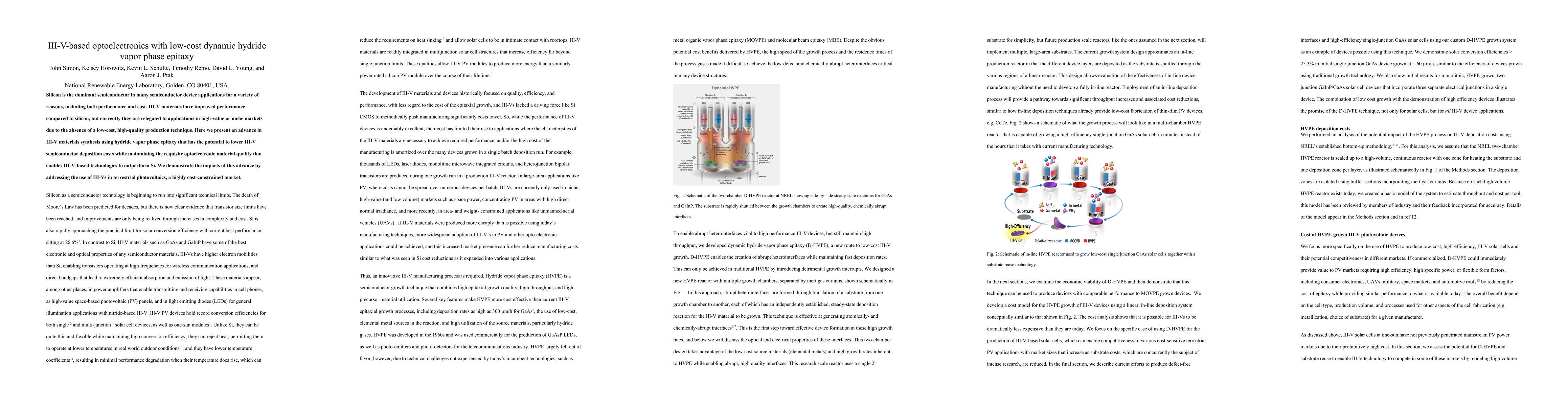
01
MethodologyHow they did it
The research methodology used a dual chamber, Dynamic-HVPE (D-HVPE) reactor to grow III-V solar cells.
This paper introduces a novel low-cost hydride vapor phase epitaxy method for synthesizing III-V materials, potentially reducing production costs significantly while preserving high optoelectronic quality. This advancement could democratize III-V-based technologies, including cost-effective terrestrial photovoltaics, and expand their use in various applications.
This paper introduces a novel low-cost hydride vapor phase epitaxy method for synthesizing III-V materials, potentially reducing production costs significantly while preserving high optoelectronic quality. This advancement could democratize III-V-based technologies, including cost-effective terrestrial photovoltaics, and expand their use in various applications.
The research methodology used a dual chamber, Dynamic-HVPE (D-HVPE) reactor to grow III-V solar cells. More in Methodology →
Main finding 1: The D-HVPE process enables high-volume growth of high-quality GaInP and GaAs layers with efficient tunnel junctions. — Main finding 2: The use of a buffer layer and ELO technology reduces substrate reuses to hundreds, while maintaining high cell efficiency. More in Key Results →
This research is important for the development of high-efficiency III-V solar cells for commercialization and large-scale deployment. More in Significance →
Limitation 1: The use of ELO technology may be challenging to scale up to hundreds of substrate reuses without compromising cell efficiency. — Limitation 2: The D-HVPE process requires significant investment in equipment and automation. More in Limitations →
Silicon is the dominant semiconductor in many semiconductor device applications for a variety of reasons, including both performance and cost. III-V materials have improved performance compared to silicon, but currently they are relegated to applications in high-value or niche markets due to the absence of a low-cost, high-quality production technique. Here we present an advance in III-V materials synthesis using hydride vapor phase epitaxy that has the potential to lower III-V semiconductor deposition costs by orders of magnitude while maintaining the requisite optoelectronic material quality that enables III-V-based technologies to outperform Si. We demonstrate the impacts of this advance by addressing the use of III-Vs in terrestrial photovoltaics, a highly cost-constrained market. The emergence of a low-cost III-V deposition technique will enable III-V electronic and opto-electronic devices, with all the benefits that they bring, to permeate throughout modern society.
Seven facets of this paper, analysed and brought into focus by AI.
This research is important for the development of high-efficiency III-V solar cells for commercialization and large-scale deployment.
The research methodology used a dual chamber, Dynamic-HVPE (D-HVPE) reactor to grow III-V solar cells.
This research is important for the development of high-efficiency III-V solar cells for commercialization and large-scale deployment.
The main technical contribution is the development and optimization of a high-volume, high-quality D-HVPE process for growing III-V solar cells with efficient tunnel junctions.
This work demonstrates the potential of D-HVPE technology for large-scale growth of high-efficiency III-V solar cells, offering a promising alternative to traditional epitaxial lift-off methods.
Current paper (gray), citations (green), references (blue)
Display is limited for performance on very large graphs.
Discussion 0