Energy dispersive X-ray spectroscopy of atomically thin semiconductors
Publication
Metrics
AI Quick Summary
This paper introduces energy dispersive X-ray spectroscopy implemented via a scanning electron microscope for atomically thin transition metal dichalcogenides, achieving layer-resolving sensitivity down to monolayers and demonstrating elemental composition profiling in heterobilayers. The method expands the characterization capabilities for two-dimensional materials and van der Waals heterostructures.
Paper Preview
Abstract
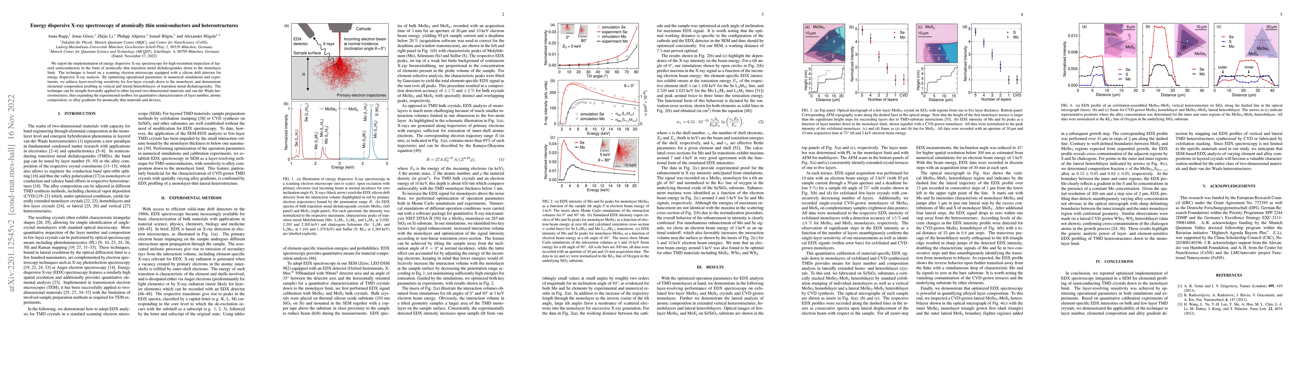
We report the implementation of energy dispersive X-ray spectroscopy for layered semiconductors in the form of atomically thin transition metal dichalcogenides. The technique is based on a scanning electron microscope equipped with a silicon drift detector for energy dispersive X-ray analysis. By optimizing operational parameters in numerical simulations and experiments, we achieve layer-resolving sensitivity for few-layer crystals down to the monolayer limit and demonstrate elemental composition profiling in vertical and lateral heterobilayers of transition metal dichalcogenides. The technique can be straight-forwardly applied to other layered two-dimensional materials and van der Waals heterostructures, thus expanding the experimental toolbox for quantitative characterization of layer number, atomic composition, or alloy gradients for atomically thin materials and devices.
AI Key Findings
Get AI-generated insights about this paper's methodology, results, significance, and more — seven facets brought into focus.
Impact
Paper Details
Authors
PDF Preview
Key Terms
Citation Network
Current paper (gray), citations (green), references (blue)
Display is limited for performance on very large graphs.
Discussion 0