Engineering and localization of quantum emitters in large hexagonal boron nitride layers

Source: ArXiv

AI Quick Summary

This paper explores the engineering and localization of quantum emitters in large hexagonal boron nitride (hBN) flakes, showing that emitters form at edges and can be activated via electron irradiation or annealing, with enhanced formation via ion implantation or laser irradiation. This discovery is crucial for advancing hBN's use in nanophotonics.

Share: Share on X LinkedIn

Summary

Hexagonal boron nitride (hBN) is a wide bandgap van der Waals material that has recently emerged as promising platform for quantum photonics experiments. In this work we study the formation and localization of narrowband quantum emitters in large flakes (up to tens of microns wide) of hBN. The emitters can be activated in as-grown hBN by electron irradiation or high temperature annealing, and the emitter formation probability can be increased by ion implantation or focused laser irradiation of the as-grown material. Interestingly, we show that the emitters are always localized at edges of the flakes, unlike most luminescent point defects in 3D materials. Our results constitute an important step on the road map of deploying hBN in nanophotonics applications.

AI Key Findings

Generated Sep 07, 2025

Methodology

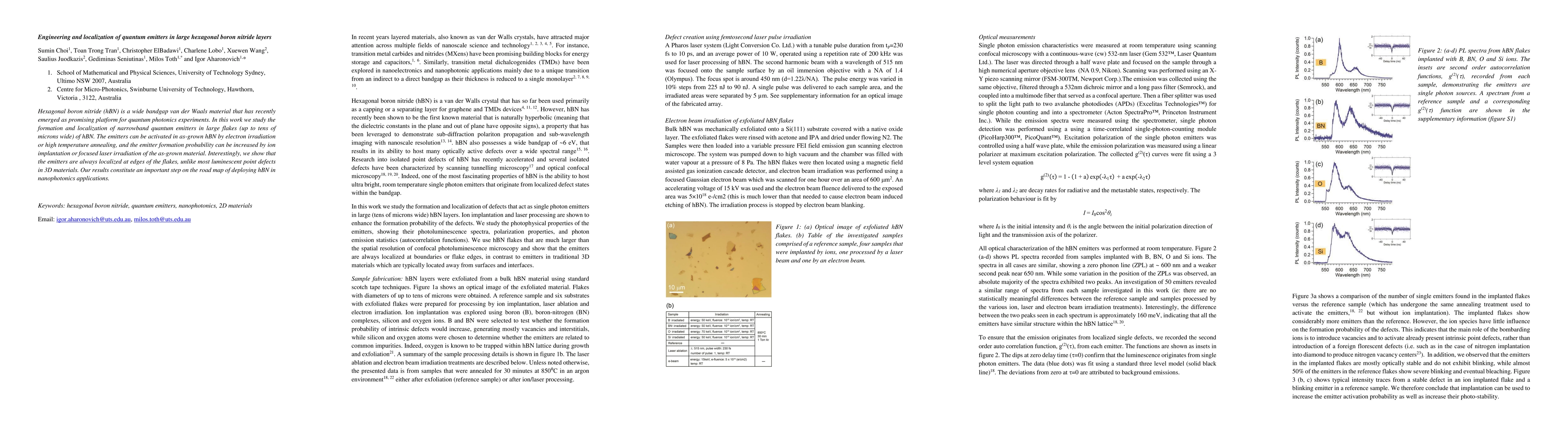
The research utilized scanning confocal microscopy with a 532-nm laser, single photon counting, and time-correlated single-photon counting for optical characterization of hBN emitters. Ion implantation, ultrafast pulsed laser processing, and electron beam irradiation were employed to fabricate the emitters in hBN flakes.

Key Results

  • Ion implantation, laser ablation, and annealing efficiently generate single photon emitters in large hBN flakes.
  • The emitters are consistently localized at flake edges, unlike most luminescent point defects in 3D materials.
  • Implantation increases emitter activation probability and photo-stability, with ion species having little influence on defect formation.

Significance

This work is significant as it presents a comprehensive study of single emitters in large layered hBN, demonstrating efficient methods for their generation and localization, which are crucial for future quantum photonics and quantum optoelectronic applications.

Technical Contribution

The paper presents a novel approach to fabricate and localize single photon emitters in large hBN flakes using ion implantation, laser processing, and electron beam irradiation techniques.

Novelty

The study distinguishes itself by demonstrating the efficient generation and localization of quantum emitters at hBN flake edges, which is an unexpected phenomenon for stable luminescent defects in semiconductors and holds promise for improved control over emitter placement in photonic and plasmonic cavities.

Limitations

  • The study did not determine whether the electron beam creates new defects or activates pre-existing ones in hBN.
  • Detailed atomistic modeling and super-resolution imaging are required to further elucidate the behavior of emitter localization at interfaces.

Future Work

  • Investigate the exact structure of single emitters in large layered hBN.
  • Explore the role of flake morphological defects in the formation of quantum emitters.

Paper Details

PDF Preview

Download PDF

Key Terms

material (0.260)
wide (0.230)
formation (0.219)
der (0.213)
annealing (0.208)
constitute (0.204)
van (0.201)
interestingly (0.194)

Citation Network

Current paper (gray), citations (green), references (blue)

Display is limited for performance on very large graphs.

Current Paper
Citations
References
Click to view
Title Authors Year Actions

Comments (0)

This website uses cookies to ensure you get the best experience. Learn more