Summary
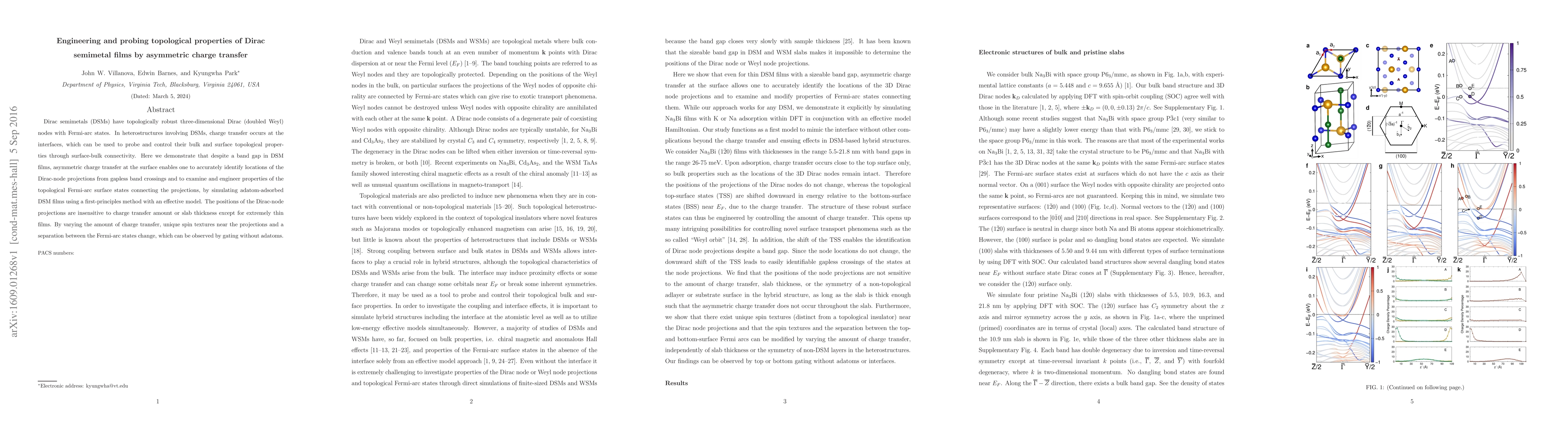
Dirac semimetals (DSMs) have topologically robust three-dimensional Dirac (doubled Weyl) nodes with Fermi-arc states. In heterostructures involving DSMs, charge transfer occurs at the interfaces, which can be used to probe and control their bulk and surface topological properties through surface-bulk connectivity. Here we demonstrate that despite a band gap in DSM films, asymmetric charge transfer at the surface enables one to accurately identify locations of the Dirac-node projections from gapless band crossings and to examine and engineer properties of the topological Fermi-arc surface states connecting the projections, by simulating adatom-adsorbed DSM films using a first-principles method with an effective model. The positions of the Dirac-node projections are insensitive to charge transfer amount or slab thickness except for extremely thin films. By varying the amount of charge transfer, unique spin textures near the projections and a separation between the Fermi-arc states change, which can be observed by gating without adatoms.
AI Key Findings
Get AI-generated insights about this paper's methodology, results, and significance.
Paper Details
PDF Preview
Key Terms
Citation Network
Current paper (gray), citations (green), references (blue)
Display is limited for performance on very large graphs.
| Title | Authors | Year | Actions |
|---|
Comments (0)