Publication
Metrics
AI Quick Summary
This paper presents a new nanofabrication technique using ion milled ultra-thin etching masks to achieve 16 nm pitch periodic structures in graphene superlattices. The method enables high-quality superlattices with a Hofstadter butterfly spectrum, potentially advancing quantum simulation and correlated electron studies.
Paper Preview
Abstract
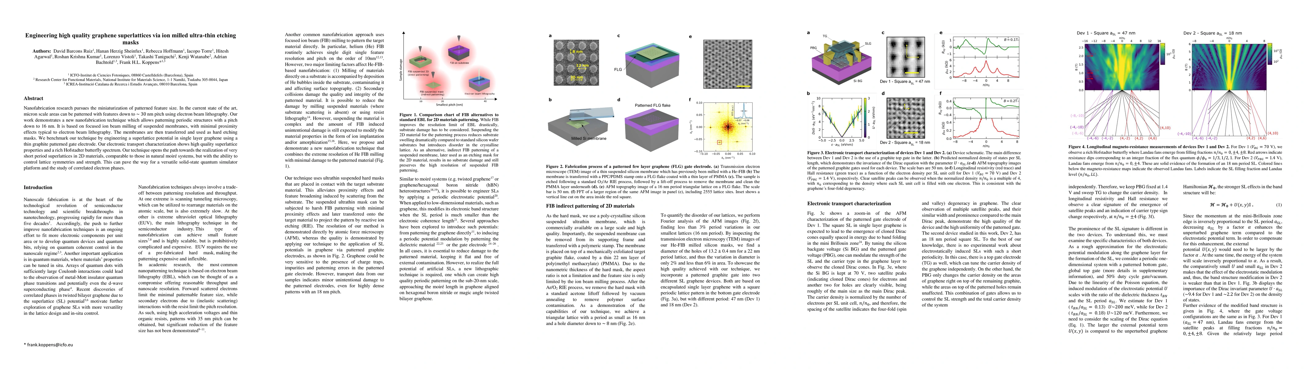
Nanofabrication research pursues the miniaturization of patterned feature size. In the current state of the art, micron scale areas can be patterned with features down to ~ 30 nm pitch using electron beam lithography. Our work demonstrates a new nanofabrication technique which allows patterning periodic structures with a pitch down to 16 nm. It is based on focused ion beam milling of suspended membranes, with minimal proximity effects typical to electron beam lithography. The membranes are then transferred and used as hard etching masks. We benchmark our technique by engineering a superlattice potential in single layer graphene using a thin graphite patterned gate electrode. Our electronic transport characterization shows high quality superlattice properties and a rich Hofstadter butterfly spectrum. Our technique opens the path towards the realization of very short period superlattices in 2D materials, comparable to those in natural moire systems, but with the ability to control lattice symmetries and strength. This can pave the way for a versatile solid-state quantum simulator platform and the study of correlated electron phases.
AI Key Findings
Get AI-generated insights about this paper's methodology, results, significance, and more — seven facets brought into focus.
Impact
Paper Details
Authors
PDF Preview
Key Terms
Citation Network
Current paper (gray), citations (green), references (blue)
Display is limited for performance on very large graphs.
Discussion 0