This study details the deposition of epitaxial Y1Ba2Cu3O7 thin films on CeO2 buffer layers on sapphire substrates using pulsed laser deposition, achieving coherent epitaxy and abrupt atomic-level interfaces. The best films exhibit a critical current of 9 e6 A/cm² at 4.2 K and lower microwave surface resistance than copper at 77 K.
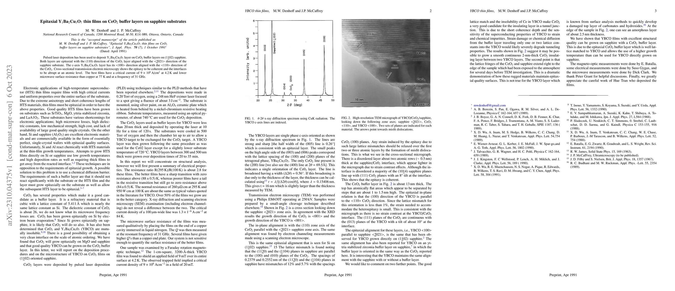
Pulsed laser deposition has been used to deposit Y1Ba2Cu3O7 layer on CeO2 buffer layers on (1102) sapphire. Both layers are epitaxial with the (110) direction of the CeO2 layer aligned with the <2021> direction of the sapphire substrate. The c-axis Y1Ba2Cu3O7 layer has its <100> direction aligned with the <110> direction of the CeO2. Cross-sectional transmission electron microscopy shows the epitaxy to be coherent and the interfaces to be abrupt at an atomic level. The best films have a critical current of 9 e6 A/cm2 at 4.2 K and lower microwave surface resistance than copper at 77 K and at a frequency of 31 GHz.
Get AI-generated insights about this paper's methodology, results, and significance.
Current paper (gray), citations (green), references (blue)
K. Andre Mkhoyan, Nitin Samarth, Yu-Sheng Huang et al.
Stephanie Law, Mingyu Yu, Lottie Murray et al.
Title | Authors | Year | Actions |
---|---|---|---|
Electrodeposition of Oriented Cerium Oxide Films
|
A. Wang, T. Golden
|
2013
|
View Paper |
Deposition of a Cu/Mo/Ce catalyst for diesel soot oxidation on a sintered metal fiber filter with a CeO2 anti corrosion coating
|
E. Bruneel, J. V. Brabant, M. T. Le, I. Driessche
|
2012
|
View Paper |
New Insights on the Intrinsic Anisotropy of YBCO Films
|
M. Al-Naafa
|
2010
|
View Paper |
Superconducting Properties of Spray Deposited TBCCO Films
|
R. Kalubarme, C. Park, S. Pawar
|
2010
|
View Paper |
YBa2Cu3O7 − δ thin films with enhanced film properties grown on sapphire using Y2O3/CeO2 bi-layer buffer
|
K. Develos-Bagarinao, H. Yamasaki
|
2009
|
View Paper |
Effect of Sputter Gas Pressure and RF Power on Surface Morphology of CeO2 Buffer Layers and Superconducting Properties of EuBa2Cu3O7-δ Thin Films by Magnetron Sputtering
|
Y. Ota, K. Kikuchi, S. Fujiwara, Yuya Unuma, Y. Kimura, O. Michikami
|
2008
|
View Paper |
Comparative studies of nanostructural and morphological evolution of CeO2 thin films induced by high-temperature annealing
|
K. Develos-Bagarinao, H. Yamasaki, Y. Nakagawa, J. Nie, M. Sohma, T. Kumagai
|
2007
|
View Paper |
Physicotechnological Principles of Deposition of Thin High-T$_{c}$ Superconducting Films of YBa$_{2}$Cu$_{3}$O$_{7-\delta}$
|
V. Flis, V. Pan, V. Komashko, V. O. Moskalyuk, I. Peshko
|
2006
|
View Paper |
Relationship between superconducting properties of EuBa2Cu3O7 thin films and surface morphology of CeO2 buffer layers on R-Al2O3
|
Y. Ota, J. Sakuma, Y. Kimura, O. Michikami
|
2006
|
View Paper |
Electrostatic spray assisted vapour deposition and structural characterisation of cerium oxide films on biaxially textured Ni tapes
|
M. Wei, D. Zhi, K. Choy
|
2006
|
View Paper |
Deposition of cerium oxide films on Si (100) and glass substrates using the ESAVD method
|
M. Wei, K. Choy
|
2005
|
View Paper |
Effect of a multi-buffer layer (Sm2O3/CeO2) on the superconducting properties of an EuBa2Cu3O7−δ thin film
|
Y. Ota, Y. Kimura, O. Michikami
|
2005
|
View Paper |
Multi-laser deposition technology for the nano-films of complex composition
|
I. Peshko, V. Flis, S. Anokhov
|
2005
|
View Paper |
Fabrication and characterization of YBCO thin film on CeO2/a-plane sapphire substrate
|
M. Shirakawa, M. Miura, T. Ohazama, Y. Shingai, A. Saito, M. Mukaida, S. Ohshima
|
2004
|
View Paper |
(1 10)Nd:KGW waveguide films grown on CeO2/Si substrates by pulsed laser deposition
|
P. Atanasov, T. Okato, R. Tomov, M. Obara
|
2004
|
View Paper |
Fabrication and characterization of a CeO2 buffer layer on c-plane and tilt-c-plane sapphire substrates
|
M. Shirakawa, J. Unno, K. Aizawa, M. Kusunoki, M. Mukaida, S. Ohshima
|
2003
|
View Paper |
Deposition of CeO2 and NiO buffer layers for YBCO coated conductors on biaxially textured Ni substrates by a MOCVD technique
|
Chan-Joong Kim, Ho-Jin Kim, Jong-Won Sun, B. Ji, Hyoung-Seop Kim, J. Joo, B. Jun, C. Jung, Soon‐Dong Park, Haiwoong Park, G. Hong
|
2003
|
View Paper |
Thallium based high temperature superconductors for microwave device applications
|
S. Speller
|
2003
|
View Paper |
TlSr2CaCu2Oy template for the growth of superconducting Tl(Ba, Sr)2Ca2Cu3Oy thin films on CeO2 buffered sapphire
|
A. Sundaresan, A. Crisan, J. Nie, M. Hirai, H. Asada, H. Kitô, Y. Tanaka, H. Ihara
|
2002
|
View Paper |
On the origin of surface outgrowths in pulsed-laser-deposited YBCO/CeO2/Al2O3 thin films
|
K. Develos, H. Yamasaki, A. Sawa, Y. Nakagawa
|
2001
|
View Paper |
Noise properties of YBa/sub 2/Cu/sub 3/O/sub 7-x/ step-edge junction dc SQUID magnetometers prepared on sapphire substrates
|
H. Lim, In-Seon Kim, Y. Park, Dongho Kim
|
2001
|
View Paper |
Superconducting properties of YBa2Cu3O7 step-edge Josephson junctions prepared on CeO2-buffered sapphire substrates
|
H. Lim, Dong Ho Kim, In-Seon Kim, Y. Park, Jong-Chul Park
|
2000
|
View Paper |
EPITAXIAL SrTiO3 BUFFER LAYERS FOR YBa2Cu3O7-δ SUPERCONDUCTING THIN FILMS ON MgO SUBSTRATE
|
Z. Mori, T. Nakagama, S. Higo, T. Doi, S. Koba, Y. Hakuraku
|
2000
|
View Paper |
Critical current density of thin YBCO films on buffered sapphire substrates
|
V. Komashko, A. Popov, V. Svetchnikov, A. Pronin, V. Melnikov, A. Galkin, V. Pan, C. Snead, M. Suenaga
|
2000
|
View Paper |
Fabrication of YBa 2Cu 3O 7 Step-Edge Junctions on Sapphire Substrates
|
In-Seon Kim, H. Lim, Dong Ho Kim, Y. Park
|
1999
|
View Paper |
Impact of microstructure on the tunability of the permittivity and the conductance of the Ba0.25Sr0.75TiO3 layer in superconductor/ferroelectric epitaxial heterostructures
|
Y. Boĭkov, T. Claeson
|
1999
|
View Paper |
Surface morphology and critical current density of high quality YBa/sub 2/Cu/sub 3/O/sub 7/ thin films on sapphire substrates
|
In-Seon Kim, H. Lim, Dongho Kim, Y. Park
|
1999
|
View Paper |
Buffers for high temperature superconductor coatings. Low temperature growth of CeO2 films by metal–organic chemical vapor deposition and their implementation as buffers
|
Anchuan Wang, J. Belot, T. Marks, P. R. Markworth, R. Chang, M. Chudzik, C. Kannewurf
|
1999
|
View Paper |
Deposition of YBCO thin films on MgO buffer layer fabricated on Si substrates
|
H. Shimakage, A. Kawakami, Z. Wang
|
1999
|
View Paper |
Epitaxial cerium oxide buffer layers and YBa_2Cu_3O_7−δ thin films for microwave device applications
|
Sissel N. Jacobsen, L. Madsen, U. Helmersson
|
1999
|
View Paper |
Epitaxial growth of YBCO thin films on Al/sub 2/O/sub 3/ substrates by pulsed laser deposition
|
In-Seon Kim, H. Lim, Y. Park
|
1999
|
View Paper |
Thallium-based HTS thin films, processing, properties and applications
|
A. Bramley, J. D. O'Connor, C. Grovenor
|
1999
|
View Paper |
The microwave power handling of an FIB-generated weak link in a YBCO film
|
A. Cowie, L. Cohen, M. Denhoff
|
1999
|
View Paper |
Effect of the laser sputtering parameters on the orientation of a cerium oxide buffer layer on sapphire and the properties of a YBa2Cu3Ox superconducting film
|
P. Mozhaev, G. Ovsyannikov, I. L. Skov
|
1999
|
View Paper |
High crystalline quality CeO2 buffer layers epitaxied on sapphire for YBa2Cu3O7 thin films
|
X. Castel, M. Guilloux-Viry, A. Perrin, J. Lesueur, F. Lalu
|
1998
|
View Paper |
YBa2Cu3O7−δ/CeO2 heterostructures on sapphire R-plane
|
Y. Boĭkov, T. Claeson, D. Erts
|
1998
|
View Paper |
Superconducting films prepared by aerosol metal organic chemical vapour deposition on substrate with buffer layer
|
K. Fröhlich, J. Šouc, A. Rosová, D. Machajdík, I. Graboy, V. Svetchnikov, A. Figueras, F. Weiss
|
1997
|
View Paper |
In-situ heteroepitaxial growth of CeO2/YBa 2Cu3O7 films on sapphire by injection CVD
|
A. Abrutis, V. Kubilius, V. Bigelytė, A. Teisˇerskis, Z. Sˇaltytė, J. Sénateur, F. Weiss
|
1997
|
View Paper |
High tunability of the permittivity of YBa2Cu3O7−∂/SrTiO3 heterostructures on sapphire substrates
|
Y. Boĭkov, T. Claeson
|
1997
|
View Paper |
Epitaxial MgO buffer layers for YBCO thin films on R-plane
|
Y. Hakuraku, K. Maezono, H. Ueda
|
1996
|
View Paper |
Deposition of CeO2 films including areas with the different orientation and sharp border between them
|
I. Kotelyanskii, V. Luzanov, Y. Dikaev, V. B. Kravchenko, B. Melekh
|
1996
|
View Paper |
Crystalline quality and surface morphology of (100) CeO2 thin films grown on sapphire substrates by solid source metalorganic chemical vapor deposition
|
Z. Lu, R. Hiskes, S. Dicarolis, A. Nel, R. Route, R. Feigelson
|
1995
|
View Paper |
Growth of pure and doped cerium oxide thin film bilayers by pulsed laser deposition
|
S. Amirhaghi, Y. Li, J. Kilner, I. Boyd
|
1995
|
View Paper |
Growth of CeO2 Films on Sapphire and MgO by rf Magnetron Sputtering
|
Wen-Chou Tsaih, Chin-Kuan Huang, T. Tseng
|
1995
|
View Paper |
The sputter deposition of cerium oxide thin films for superconducting electronics
|
J. Owens, E. Tarte, P. Berghuis, R. Somekh
|
1995
|
View Paper |
Control of CeO2 growth by metalorganic chemical vapor deposition with a special source evaporator
|
S. Liang, C. Chern, Z. Shi, P. Lu, Yicheng Lu, B. Kear
|
1995
|
View Paper |
A spectroscopic ellipsometry study of cerium dioxide thin films grown on sapphire by rf magnetron sputtering
|
S. Guo, H. Arwin, S. N. Jacobsen, K. Järrendahl, U. Helmersson
|
1995
|
View Paper |
Reduced YSZ deposition temperatures for YBa_2Cu_3O_x/YSZ thin films on sapphire
|
J. Kroese, A. J. Drehrman, J. Horrigan
|
1995
|
View Paper |
Epitaxial Growth and AFM Observation of YBCO/CeO2/Al2O3 Films
|
Yoshitaka Nakamura, Hitoshi Kohno, S. Ohshima, K. Okuyama, H. Myoren, Tsutomu Yamasita, H. Yamane, T. Hirai
|
1995
|
View Paper |
Surface crystallographic structure compatibility between substrates and high T_c (YBCO) thin films
|
R. Guo, A. Bhalla, L. Cross, R. Roy
|
1994
|
View Paper |
Deposition of CeO2 on Si(111) studied by LEED, AES, XPS and RBS
|
C. Guillaume, M. Vermeersch, R. Sporken, J. Verbist, S. Mathot, G. Demortier
|
1994
|
View Paper |
YBa2Cu3O7−δ-thin films on sapphire with buffer layers of CeO2
|
M. Maul, B. Schulte, P. Häussler, H. Adrian
|
1994
|
View Paper |
Investigation of substrate temperature effect on the surface morphology of excimer laser deposited YBa2Cu3O7/CeO2 films on sapphire
|
P. Grant, H. Tran, M. Denhoff
|
1994
|
View Paper |
Epitaxial CeO2 buffer layers for YBa2Cu3O7−δ films on sapphire
|
M. Maul, B. Schulte, P. Häussler, G. Frank, T. Steinborn, H. Fuess,, H. Adrian
|
1993
|
View Paper |
Cerium dioxide thin film optical waveguides
|
P. Wahid, K. Sundaram, P. Sisk
|
1992
|
View Paper |
Accelerated formation of the high-Tc phase in moderately Pb doped BiSrCaCuO thin films
|
L. Phong, B. Tremblay, I. Shih, C. X. Qiu
|
1992
|
View Paper |
Small-angle cleavage of semiconductors for transmission electron microscopy
|
J. McCaffrey
|
1991
|
View Paper |
Thermal boundary resistance in YBCO THz microbolometers at room temperature
|
P. Herman
|
2014
|
View Paper |
Fabrication process of YBCO thin film starting from amorphous film for microstrip line device
|
J. Muyari, N. Kobayashi, S. Takahashi, K. Hayashi, A. Saito, S. Ohshima
|
2012
|
View Paper |
Low-Temperature Anode-Supported SOFC with Ultra-Thin Ceria-Based Electrolytes Prepared by Modified Sol—Gel Route
|
Hongfei Lin, C. Ding, Kazuhisa Sato, Yoshifumi Tsutai, T. Hashida
|
2010
|
View Paper |
EuBa2Cu3O7-δ 薄膜用 CeO2 バッファ層に対するスパッタガス圧の効果
|
聡子 藤原, 靖之 太田, 豊 木村, 裕也 宇沼, 啓太 作間, 修 道上
|
2008
|
View Paper |
R-Al2O3基板上EuBa2Cu3O7-δ薄膜の超伝導特性及び結晶成長に対する厚膜CeO2バッファ層の表面性状の影響
|
靖之 太田, 純子 佐久間, 豊 木村, 修 道上
|
2006
|
View Paper |
Structural and electrical properties of cerium dioxide films grown by RF magnetron sputtering
|
W. Tsai, T. Tseng
|
1997
|
View Paper |
Fabrication and Characterization of Heteroepitaxial YBCO/CeO2/Al2O3 Films
|
Yoshitaka Nakamura, Akira Ohsuka, S. Ohshima, K. Okuyama
|
1996
|
View Paper |
Afm Study of CeO 2 Growth on Sapphire as a Buffer Layer for YBa 2 Cu 3 O 7
|
M. Denhoff, B. Mason, H. Tran, P. Grant
|
1995
|
View Paper |
Sputtered and Reactively Grown Epitaxial GdAIO3 Films as Buffer Layers for C-Oriented YBa2Cu3O7-δ Films on R-Sapphire
|
S. Senz, H. Sieber, N. Zakharov, M. Lorenz, H. Hochmuth, D. Hesse
|
1995
|
View Paper |
Deposition of Cerium Dioxide Thin Films on Silicon Substrates by Atomic Layer Epitaxy
|
H. Mölsä, L. Niinistö
|
1993
|
View Paper |
Growth of Cerium Oxide Buffer Layers and Superconducting thin films on Silicon
|
S. Amirhaghi, F. Beech, V. Craciun, A. Sajjadi, M. Vickers, S. Tarling, P. Barnes, W. Andboydi
|
1992
|
View Paper |
Comments (0)