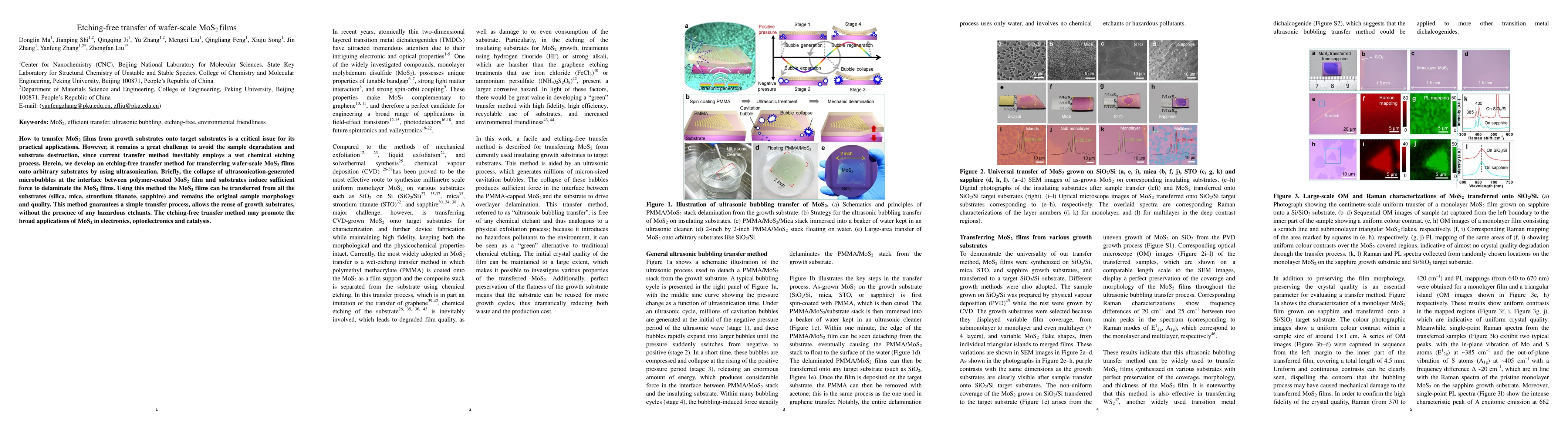
Publication
Metrics
AI Quick Summary
This paper introduces an etching-free ultrasonication method to transfer wafer-scale MoS2 films onto various substrates without degrading the sample or damaging the growth substrate, potentially expanding MoS2's applications in electronics and optoelectronics. The technique uses microbubble collapse induced by ultrasonication to delaminate MoS2 films while preserving their original morphology and quality.
Paper Preview
Abstract
How to transfer MoS2 films from growth substrates onto target substrates is a critical issue for its practical applications. However, it remains a great challenge to avoid the sample degradation and substrate destruction, since current transfer method inevitably employs a wet chemical etching process. Herein, we develop an etching-free transfer method for transferring wafer-scale MoS2 films onto arbitrary substrates by using ultrasonication. Briefly, the collapse of ultrasonication-generated microbubbles at the interface between polymer-coated MoS2 film and substrates induce sufficient force to delaminate the MoS2 films. Using this method the MoS2 films can be transferred from all the substrates (silica, mica, strontium titanate, sapphire) and remains the original sample morphology and quality. This method guarantees a simple transfer process, allows the reuse of growth substrates, without the presence of any hazardous etchants. The etching-free transfer method may promote the broad applications of MoS2 in electronics, optoelectronics and catalysis.
AI Key Findings
Get AI-generated insights about this paper's methodology, results, significance, and more — seven facets brought into focus.
Impact
Paper Details
PDF Preview
Key Terms
Citation Network
Current paper (gray), citations (green), references (blue)
Display is limited for performance on very large graphs.
Discussion 0