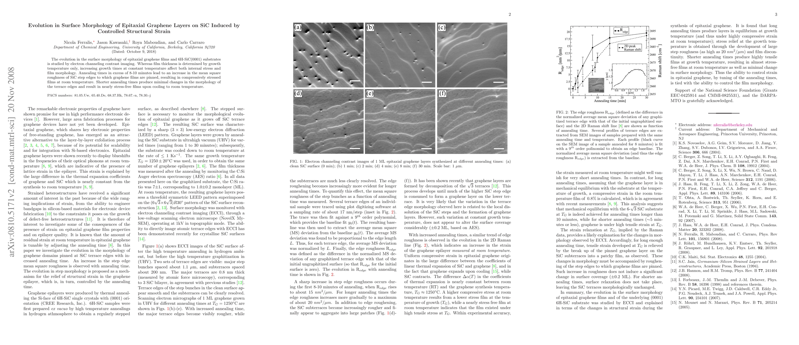
This study investigates how controlled structural strain affects the surface morphology of epitaxial graphene films on 6H-SiC substrates, revealing that increased annealing times lead to higher mean square roughness of SiC step edges, resulting in compressively stressed graphene films at room temperature. Shorter annealing times maintain minimal changes in terrace edges, yielding nearly stress-free films upon cooling.
The evolution in the surface morphology of epitaxial graphene films and 6H-SiC(0001) substrates is studied by electron channeling contrast imaging. Whereas film thickness is determined by growth temperature only, increasing growth times at constant temperature affect both internal stress and film morphology. Annealing times in excess of 8-10 minutes lead to an increase in the mean square roughness of SiC step edges to which graphene films are pinned, resulting in compressively stressed films at room temperature. Shorter annealing times produce minimal changes in the morphology of the terrace edges and result in nearly stress-free films upon cooling to room temperature.
Get AI-generated insights about this paper's methodology, results, and significance.
Current paper (gray), citations (green), references (blue)
Title | Authors | Year | Actions |
---|---|---|---|
Stacking domain morphology in epitaxial graphene on silicon carbide
|
Tobias A. de Jong, L. Visser, J. Jobst, R. Tromp, S. V. D. Molen
|
2022
|
View Paper |
Sub-boundaries induced by dislocational creep in uranium dioxide analyzed by advanced diffraction and channeling electron microscopy
|
M. Saada, N. Gey, B. Beausir, X. Iltis, H. Mansour, N. Maloufi
|
2017
|
View Paper |
Formation of graphite/sic structures by the thermal decomposition of silicon carbide
|
M. Mynbaeva, A. Lavrent’ev, K. Mynbaev
|
2016
|
View Paper |
Characterization of SiC-grown epitaxial graphene microislands using tip-enhanced Raman spectroscopy.
|
S. Vantasin, Yoshito Y. Tanaka, Shohei Uemura, Toshiaki Suzuki, Yasunori Kutsuma, Daichi Doujima, T. Kaneko, Y. Ozaki
|
2015
|
View Paper |
Sub-micron resolution selected area electron channeling patterns.
|
J. Guyon, H. Mansour, N. Gey, M. Crimp, Smail Chalal, N. Maloufi
|
2015
|
View Paper |
Graphene Manipulation on 4H-SiC(0001) Using Scanning Tunneling Microscopy
|
P. Xu, M. Ackerman, S. Barber, J. K. Schoelz, D. Qi, P. Thibado, V. Wheeler, L. Nyakiti, R. Myers-Ward, Charles R. Eddy, Jr., D. Gaskill
|
2015
|
View Paper |
Evolution of interfacial intercalation chemistry on epitaxial graphene/SiC by surface enhanced Raman spectroscopy
|
N. Ferralis, C. Carraro
|
2014
|
View Paper |
Accurate electron channeling contrast analysis of dislocations in fine grained bulk materials
|
H. Mansour, J. Guyon, M. Crimp, N. Gey, B. Beausir, N. Maloufi
|
2014
|
View Paper |
The correlation of epitaxial graphene properties and morphology of SiC (0001)
|
Yongquan Guo, Liwei Guo, J. Huang, R. Yang, Y. Jia, Jingjing Lin, W. Lu, Z. L. Li, Xiaolong Chen
|
2014
|
View Paper |
Looking behind the scenes: Raman spectroscopy of top-gated epitaxial graphene through the substrate
|
F. Fromm, P. Wehrfritz, M. Hundhausen, T. Seyller
|
2013
|
View Paper |
Competing scanning tunneling microscope tip-interlayer interactions for twisted multilayer graphene on the a-plane SiC surface
|
P. Xu, M. Ackerman, S. Barber, J. K. Schoelz, P. Thibado, V. Wheeler, L. Nyakiti, R. Myers-Ward, C. Eddy, D. Gaskill
|
2013
|
View Paper |
Atomic-scale movement induced in nanoridges by scanning tunneling microscopy on epitaxial graphene grown on 4H-SiC(0001)
|
P. Xu, S. Barber, J. K. Schoelz, M. Ackerman, D. Qi, P. Thibado, V. Wheeler, L. Nyakiti, R. Myers-Ward, C. Eddy, D. Gaskill
|
2013
|
View Paper |
The influence of substrate morphology on thickness uniformity and unintentional doping of epitaxial graphene on SiC
|
J. Eriksson, R. Pearce, T. Iakimov, C. Virojanadara, D. Gogova, M. Andersson, M. Syväjärvi, A. Spetz, R. Yakimova
|
2012
|
View Paper |
Preparation of Quasi-Free-Standing Graphene with a Super Large Interlayer Distance by Methane Intercalation
|
Qingsong Huang, XL(陈西良) Chen, Jj Lin, Kang Li, Y. Jia, Jun Liu, L. Guo, Wj Wang, Gang Wang
|
2011
|
View Paper |
Graphene epitaxy by chemical vapor deposition on SiC.
|
W. Strupinski, K. Grodecki, A. Wysmołek, R. Stępniewski, T. Szkopek, P. Gaskell, Alexander Grüneis, Alexander Grüneis, D. Haberer, R. Bożek, Jerzy Krupka, J. Baranowski
|
2011
|
View Paper |
Probing mechanical properties of graphene with Raman spectroscopy
|
N. Ferralis
|
2010
|
View Paper |
Anisotropic transport in graphene on SiC substrate with periodic nanofacets
|
S. Odaka, H. Miyazaki, Song-Lin Li, A. Kanda, K. Morita, Satoru Tanaka, Y. Miyata, H. Kataura, K. Tsukagoshi, Y. Aoyagi
|
2010
|
View Paper |
Atomic scale flattening, step formation and graphitization blocking on 6H- and 4H-SiC{0 0 0 1} surfaces under Si flux
|
F. Ferrer, E. Moreau, D. Vignaud, S. Godey, X. Wallart
|
2009
|
View Paper |
Atomic-scale imaging and manipulation of ridges on epitaxial graphene on 6H-SiC(0001)
|
G. Sun, G. Sun, Juanjuan Jia, Juanjuan Jia, Q. Xue, Q. Xue, Lian Li
|
2009
|
View Paper |
Sub-boundaries induced by dislocational creep in uranium dioxide analyzed by advanced di ff raction and channeling electron microscopy
|
M. B. Saadaa, N. Geya, B. Beausira, X. Iltisb, H. Mansoura, N. Malou
|
2017
|
View Paper |
Characterization of wide band gap semiconductors using electron channeling contrast imaging: A review of applications and potential
|
J. Hite
|
2014
|
View Paper |
Comments (0)