Publication
Metrics
AI Quick Summary
This paper details a wafer-scale tunnel junction fabrication method using plasma etching and ex-situ oxidation, achieving a local resistance deviation below 7.5%. Sub-1 K measurements and Coulomb blockade thermometry reveal an upper limit of ~5% deviation for the junction array, comparable to the experimental setup's accuracy.
Paper Preview
Abstract
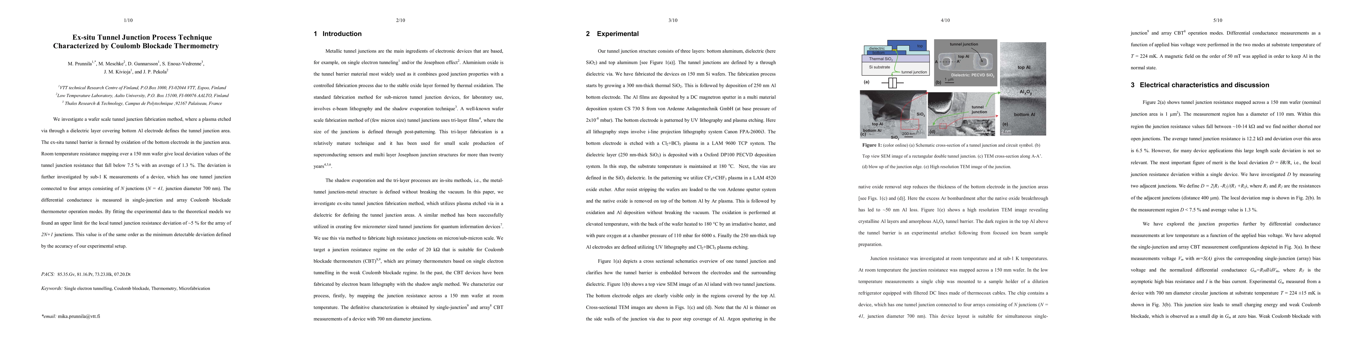
We investigate a wafer scale tunnel junction fabrication method, where a plasma etched via through a dielectric layer covering bottom Al electrode defines the tunnel junction area. The ex-situ tunnel barrier is formed by oxidation of the bottom electrode in the junction area. Room temperature resistance mapping over a 150 mm wafer give local deviation values of the tunnel junction resistance that fall below 7.5 % with an average of 1.3 %. The deviation is further investigated by sub-1 K measurements of a device, which has one tunnel junction connected to four arrays consisting of N junctions (N = 41, junction diameter 700 nm). The differential conductance is measured in single-junction and array Coulomb blockade thermometer operation modes. By fitting the experimental data to the theoretical models we found an upper limit for the local tunnel junction resistance deviation of ~5 % for the array of 2N+1 junctions. This value is of the same order as the minimum detectable deviation defined by the accuracy of our experimental setup.
AI Key Findings
Get AI-generated insights about this paper's methodology, results, significance, and more — seven facets brought into focus.
Impact
Paper Details
PDF Preview
Key Terms
Citation Network
Current paper (gray), citations (green), references (blue)
Display is limited for performance on very large graphs.
Discussion 0