Summary
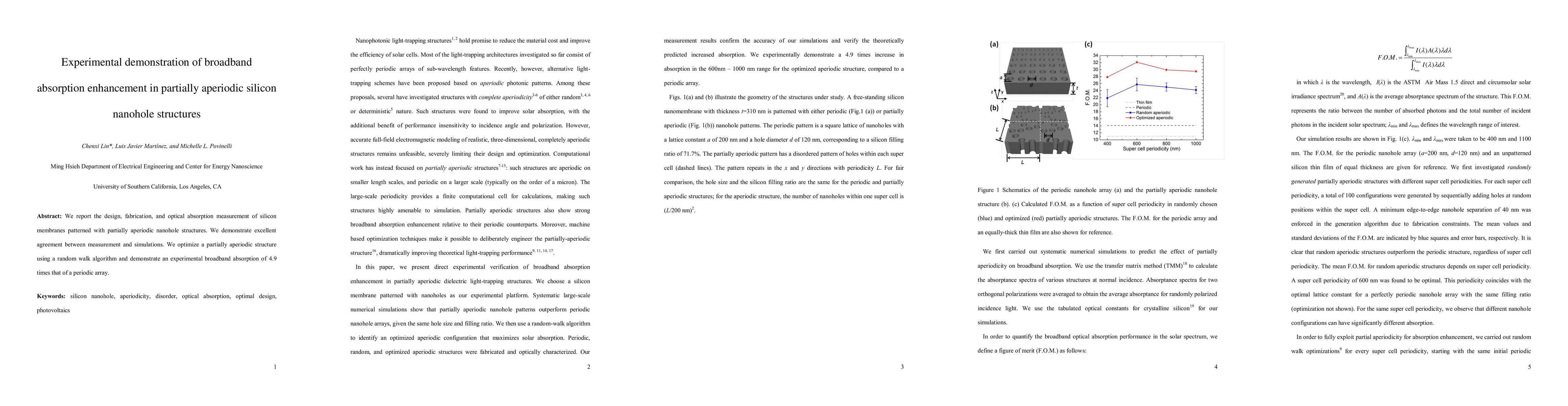
We report the design, fabrication, and optical absorption measurement of silicon membranes patterned with partially aperiodic nanohole structures. We demonstrate excellent agreement between measurement and simulations. We optimize a partially aperiodic structure using a random walk algorithm and demonstrate an experimental broadband absorption of 4.9 times that of a periodic array.
AI Key Findings
Get AI-generated insights about this paper's methodology, results, and significance.
Paper Details
PDF Preview
Key Terms
partially
(0.339)
absorption
(0.305)
measurement
(0.271)
fabrication
(0.237)
random walk
(0.231)
excellent agreement
(0.231)
broadband
(0.228)
walk
(0.221)
Citation Network
Current paper (gray), citations (green), references (blue)
Display is limited for performance on very large graphs.
Current Paper
Citations
References
Click to view
Similar Papers
Found 4 papers| Title | Authors | Year | Actions |
|---|
Comments (0)