Publication
Metrics
AI Quick Summary
This paper reports on both numerical simulations and experimental measurements of the optical response of a gold nanostrip in a silicon waveguide gap, revealing distinct spectral features compared to free-space excitation due to interference between the guided field and the nanostructure's electric dipolar resonance, leading to high-contrast Fano profiles and a notable transmission/reflection crossing. This approach may enable advanced on-chip applications in biosensing and optical switching.
Paper Preview
Abstract
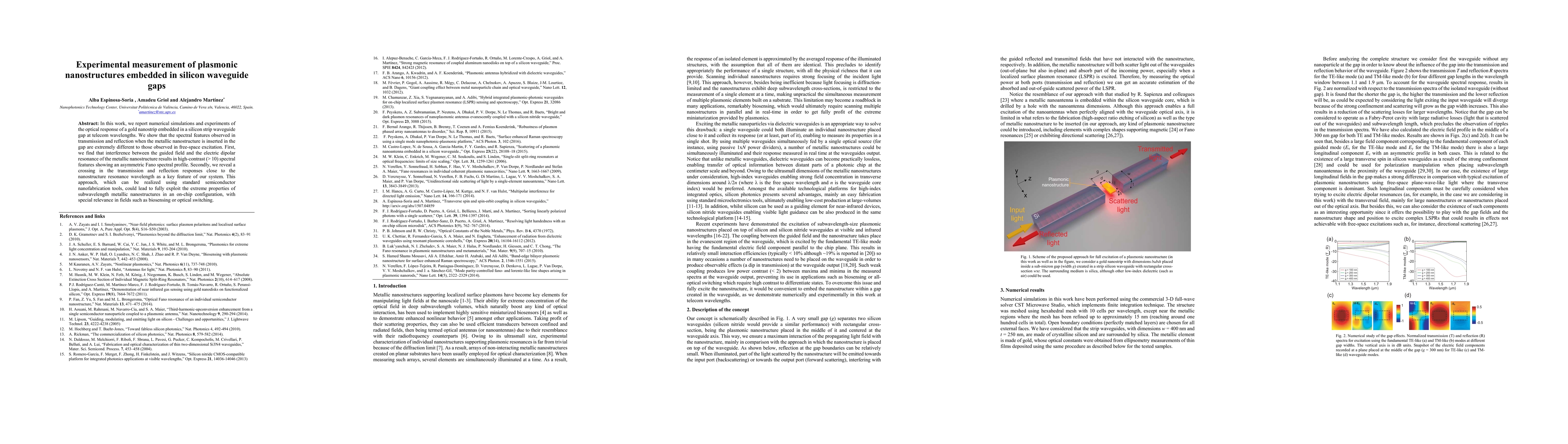
In this work, we report numerical simulations and experiments of the optical response of a gold nanostrip embedded in a silicon strip waveguide gap at telecom wavelengths. We show that the spectral features observed in transmission and reflection when the metallic nanostructure is inserted in the gap are extremely different to those observed in free-space excitation. First, we find that interference between the guided field and the electric dipolar resonance of the metallic nanostructure results in high-contrast (> 10) spectral features showing an asymmetric Fano spectral profile. Secondly, we reveal a crossing in the transmission and reflection responses close to the nanostructure resonance wavelength as a key feature of our system. This approach, which can be realized using standard semiconductor nanofabrication tools, could lead to fully exploit the extreme properties of subwavelength metallic nanostructures in an on-chip configuration, with special relevance in fields such as biosensing or optical switching.
AI Key Findings
Get AI-generated insights about this paper's methodology, results, significance, and more — seven facets brought into focus.
Impact
Paper Details
PDF Preview
Key Terms
Citation Network
Current paper (gray), citations (green), references (blue)
Display is limited for performance on very large graphs.
Discussion 0