Publication
Metrics
AI Quick Summary
This paper reports the experimental realization of an electronic Lieb lattice using surface state electrons on Cu(111) confined by CO molecules, confirmed via scanning tunneling microscopy and spectroscopy. The study reveals the predicted electronic structure, including Dirac cones and a topological flat band, corroborated by theoretical calculations.
Paper Preview
Abstract
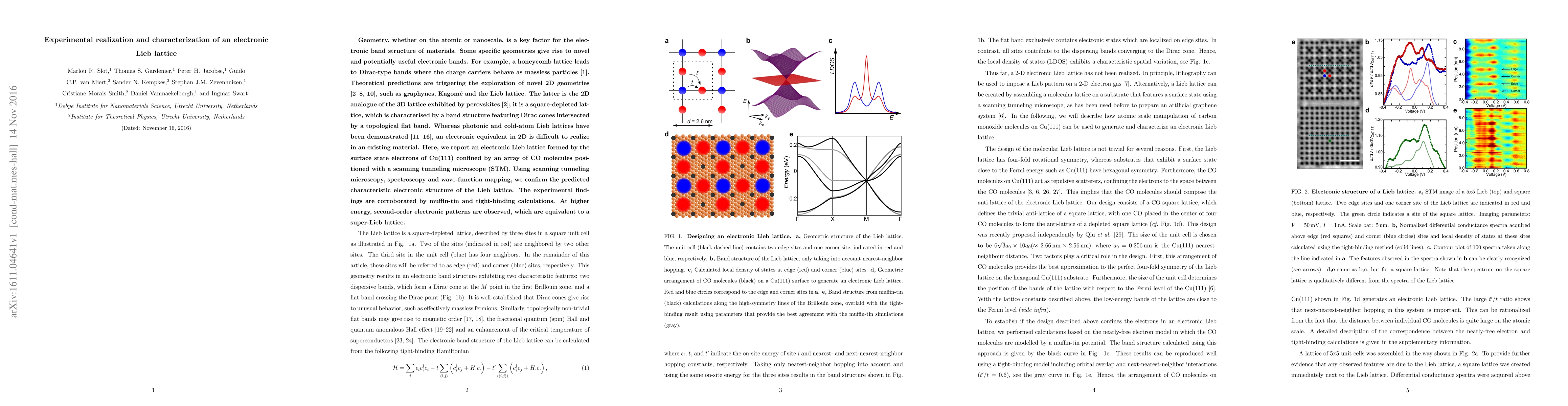
Geometry, whether on the atomic or nanoscale, is a key factor for the electronic band structure of materials. Some specific geometries give rise to novel and potentially useful electronic bands. For example, a honeycomb lattice leads to Dirac-type bands where the charge carriers behave as massless particles. Theoretical predictions are triggering the exploration of novel 2D geometries, such as graphynes, Kagom\'{e} and the Lieb lattice. The latter is the 2D analogue of the 3D lattice exhibited by perovskites; it is a square-depleted lattice, which is characterised by a band structure featuring Dirac cones intersected by a topological flat band. Whereas photonic and cold-atom Lieb lattices have been demonstrated, an electronic equivalent in 2D is difficult to realize in an existing material. Here, we report an electronic Lieb lattice formed by the surface state electrons of Cu(111) confined by an array of CO molecules positioned with a scanning tunneling microscope (STM). Using scanning tunneling microscopy, spectroscopy and wave-function mapping, we confirm the predicted characteristic electronic structure of the Lieb lattice. The experimental findings are corroborated by muffin-tin and tight-binding calculations. At higher energy, second-order electronic patterns are observed, which are equivalent to a super-Lieb lattice.
AI Key Findings
Get AI-generated insights about this paper's methodology, results, significance, and more — seven facets brought into focus.
Impact
Paper Details
PDF Preview
Key Terms
Citation Network
Current paper (gray), citations (green), references (blue)
Display is limited for performance on very large graphs.
Discussion 0