Experimental realization of single electron tunneling diode based on vertical graphene two-barrier junction
Publication
Metrics
Paper Preview
Abstract
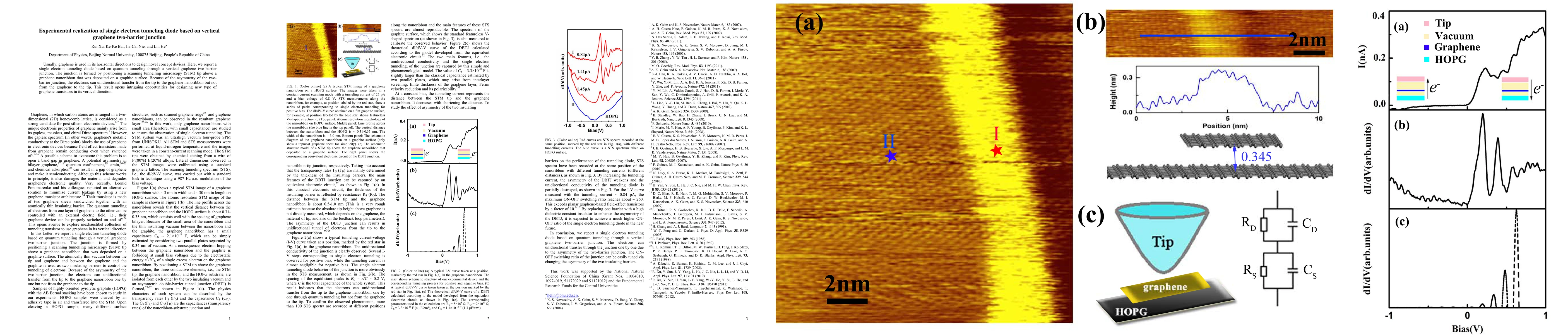
Usually, graphene is used in its horizontal directions to design novel concept devices. Here, we report a single electron tunneling diode based on quantum tunneling through a vertical graphene two-barrier junction. The junction is formed by positioning a scanning tunnelling microscopy (STM) tip above a graphene nanoribbon that was deposited on a graphite surface. Because of the asymmetry of the two-barrier junction, the electrons can unidirectional transfer from the tip to the graphene nanoribbon but not from the graphene to the tip. This result opens intriguing opportunities for designing new type of graphene transistors in its vertical direction.
AI Key Findings
Get AI-generated insights about this paper's methodology, results, significance, and more — seven facets brought into focus.
Paper Details
PDF Preview
Key Terms
Related Papers
No references found for this paper.
Discussion 0