Explicit Gain Equations for Single Crystalline Photoconductors
Publication
Metrics
Paper Preview
Abstract
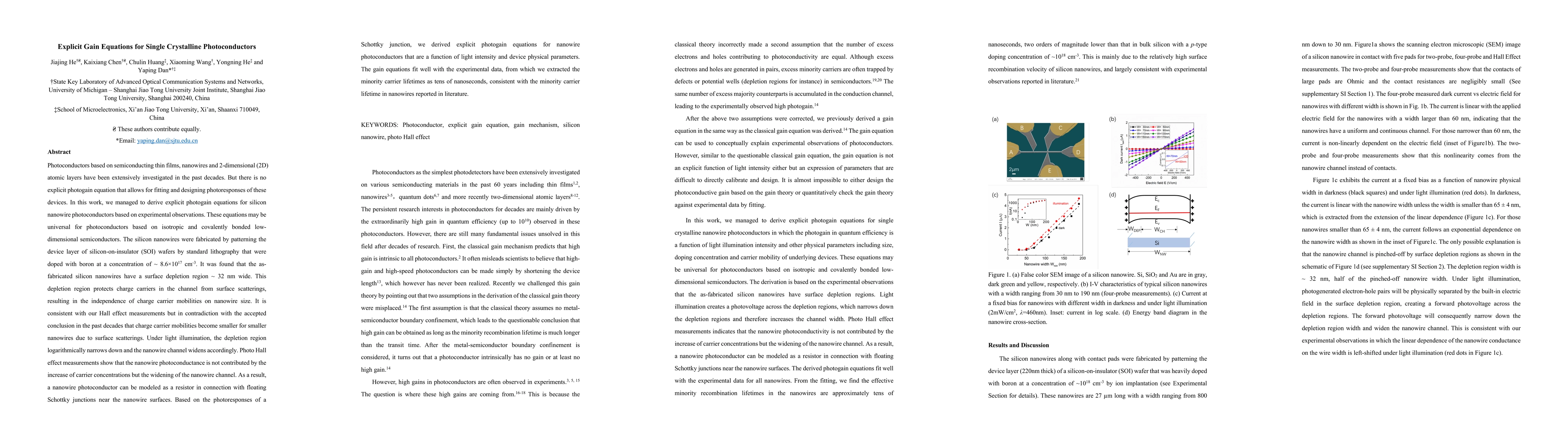
Photoconductors based on semiconducting thin films, nanowires and 2-dimensional atomic layers have been extensively investigated. But there is no explicit photogain equation that allows for fitting and designing photoresponses of these devices. In this work, we managed to derive explicit photogain equations for silicon nanowire photoconductors based on experimental observations. The silicon nanowires were fabricated by patterning the device layer of silicon-on-insulator wafers by standard lithography that were doped with boron. It was found that the as-fabricated silicon nanowires have a surface depletion region ~ 32 nm wide. This depletion region protects charge carriers in the channel from surface scatterings, resulting in the independence of charge carrier mobilities on nanowire size. It is consistent with our Hall effect measurements but in contradiction with the accepted conclusion in the past decades that charge carrier mobilities become smaller for smaller nanowires due to surface scatterings. Under light illumination, the depletion region logarithmically narrows down and the nanowire channel widens accordingly. Photo Hall effect measurements show that the nanowire photoconductance is not contributed by the increase of carrier concentrations but the widening of the nanowire channel. As a result, a nanowire photoconductor can be modeled as a resistor in connection with floating Schottky junctions near the nanowire surfaces. Based on the photoresponses of a Schottky junction, we derived explicit photogain equations for nanowire photoconductors that are a function of light intensity and device physical parameters. The gain equations fit well with the experimental data, from which we extracted the minority carrier lifetimes that are consistent with the minority carrier lifetime in nanowires reported in literature.
AI Key Findings
Get AI-generated insights about this paper's methodology, results, significance, and more — seven facets brought into focus.
Impact
Paper Details
Authors
PDF Preview
Key Terms
Citation Network
Current paper (gray), citations (green), references (blue)
Display is limited for performance on very large graphs.
Discussion 0