Exploring possibilities of band gap measurement with off-axis EELS in TEM
Publication
Metrics
AI Quick Summary
This paper presents a novel technique using off-axis EELS in TEM to measure the band gap of dielectric materials with high refractive indices, employing a Bessel aperture to enhance signal-to-noise ratio and selectivity of transitions from valence to conduction bands. Experimental results on diamond, GaN, and AlN demonstrate the method's effectiveness.
Paper Preview
Abstract
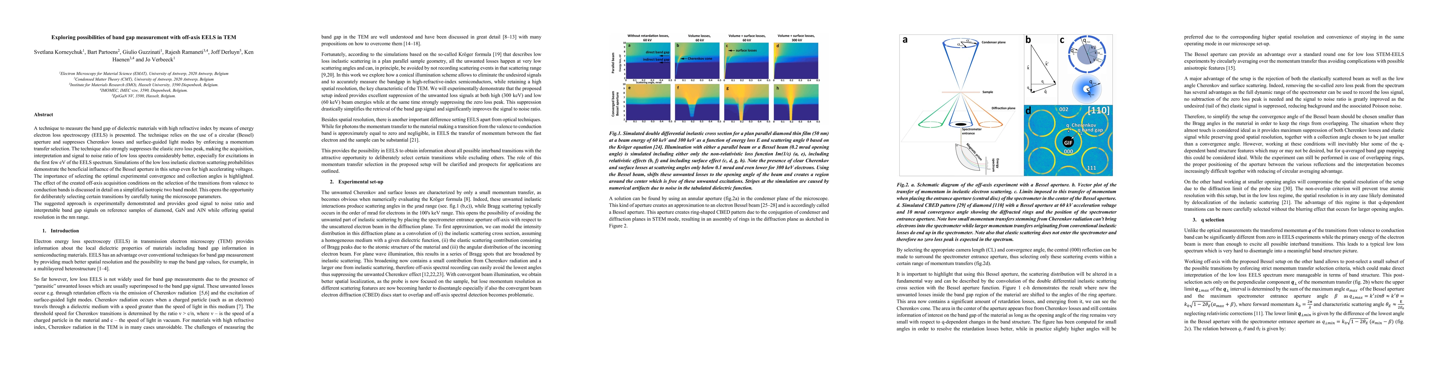
A technique to measure the band gap of dielectric materials with high refractive index by means of energy electron loss spectroscopy (EELS) is presented. The technique relies on the use of a circular (Bessel) aperture and suppresses Cherenkov losses and surface-guided light modes by enforcing a momentum transfer selection. The technique also strongly suppresses the elastic zero loss peak, making the acquisition, interpretation and signal to noise ratio of low loss spectra considerably better, especially for excitations in the first few eV of the EELS spectrum. Simulations of the low loss inelastic electron scattering probabilities demonstrate the beneficial influence of the Bessel aperture in this setup even for high accelerating voltages. The importance of selecting the optimal experimental convergence and collection angles is highlighted. The effect of the created off-axis acquisition conditions on the selection of the transitions from valence to conduction bands is discussed in detail on a simplified isotropic two band model. This opens the opportunity for deliberately selecting certain transitions by carefully tuning the microscope parameters. The suggested approach is experimentally demonstrated and provides good signal to noise ratio and interpretable band gap signals on reference samples of diamond, GaN and AlN while offering spatial resolution in the nm range.
AI Key Findings
Get AI-generated insights about this paper's methodology, results, significance, and more — seven facets brought into focus.
Impact
Paper Details
PDF Preview
Key Terms
Citation Network
Current paper (gray), citations (green), references (blue)
Display is limited for performance on very large graphs.
Discussion 0