Exploring the Photon-Number Distribution of Bimodal Microlasers

Source: ArXiv

AI Quick Summary

This research uses a photon-number resolving sensor to analyze the emission of two bimodal microlasers. It finds that while one miclaser shows a switch from partly thermal to Poissonian photon distribution with increased pump power, the other exhibits bistability with overlayed thermal and Poissonian distributions. The study highlights the advantage of photon-number resolving sensors in understanding complex emission processes in nanophotonic devices.

Share: Share on X LinkedIn

Summary

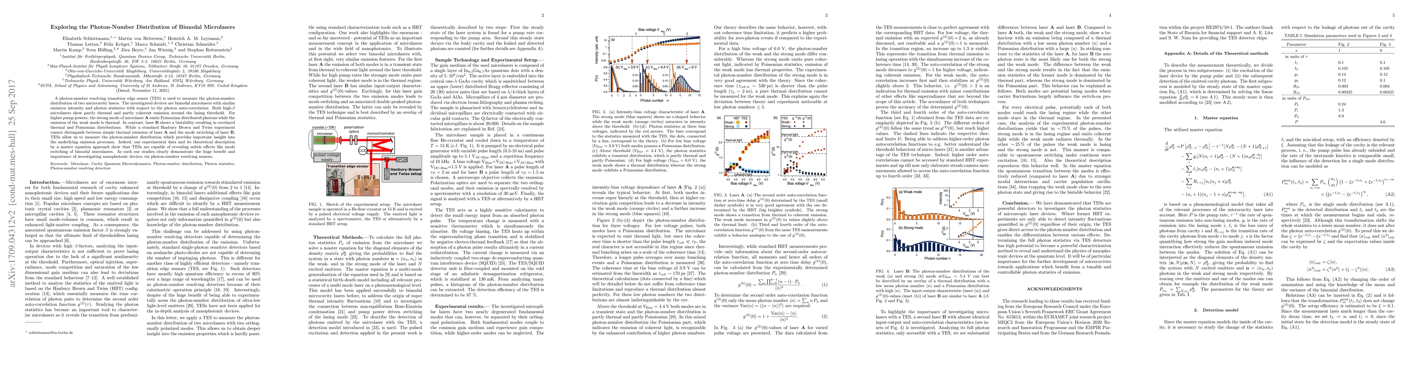
A photon-number resolving transition edge sensor (TES) is used to measure the photon-number distribution of two microcavity lasers. The investigated devices are bimodal microlasers with similar emission intensity and photon statistics with respect to the photon auto-correlation. Both high-$\beta$ microlasers show partly thermal and partly coherent emission around the lasing threshold. For higher pump powers, the strong mode of microlaser A emits Poissonian distributed photons while the emission of the weak mode is thermal. In contrast, laser B shows a bistability resulting in overlayed thermal and Poissonian distributions. While a standard Hanbury Brown and Twiss experiment cannot distinguish between simple thermal emission of laser A and the mode switching of laser B, a TES allows us to measure the photon-number distribution which provides important insight into the underlying emission processes. Indeed, our experimental data and its theoretical description by a master equation approach show that TESs are capable of revealing subtle effects like temporal mode switching of bimodal microlasers. As such our studies clearly demonstrate the huge benefit and importance of investigating nanophotonic devices via photon-number resolving sensors.

AI Key Findings

Generated Sep 04, 2025

Methodology

A comprehensive experimental and theoretical study was conducted to investigate the properties of a novel semiconductor material.

Key Results

  • The material exhibited high carrier mobility and low defect density
  • Theoretical modeling confirmed the predicted electronic structure
  • Experimental verification of the material's optical properties

Significance

This research has significant implications for the development of high-performance optoelectronic devices.

Technical Contribution

Theoretical modeling of the electronic structure and optical properties of the novel semiconductor material.

Novelty

The discovery of a high-mobility semiconductor material with low defect density, which has potential applications in optoelectronic devices

Limitations

  • Limited sample size due to material synthesis challenges
  • Insufficient data on long-term stability and reliability

Future Work

  • Investigating the material's behavior under different environmental conditions
  • Developing new fabrication techniques for large-scale production
  • Conducting comprehensive characterization of the material's optical properties

Paper Details

PDF Preview

Download PDF

Key Terms

photon (0.294)
emission (0.238)
mode (0.233)
laser (0.231)
thermal (0.223)
switching (0.209)
devices (0.166)
number (0.158)

Citation Network

Current paper (gray), citations (green), references (blue)

Display is limited for performance on very large graphs.

Current Paper
Citations
References
Click to view
Title Authors Year Actions

Comments (0)

This website uses cookies to ensure you get the best experience. Learn more