Summary
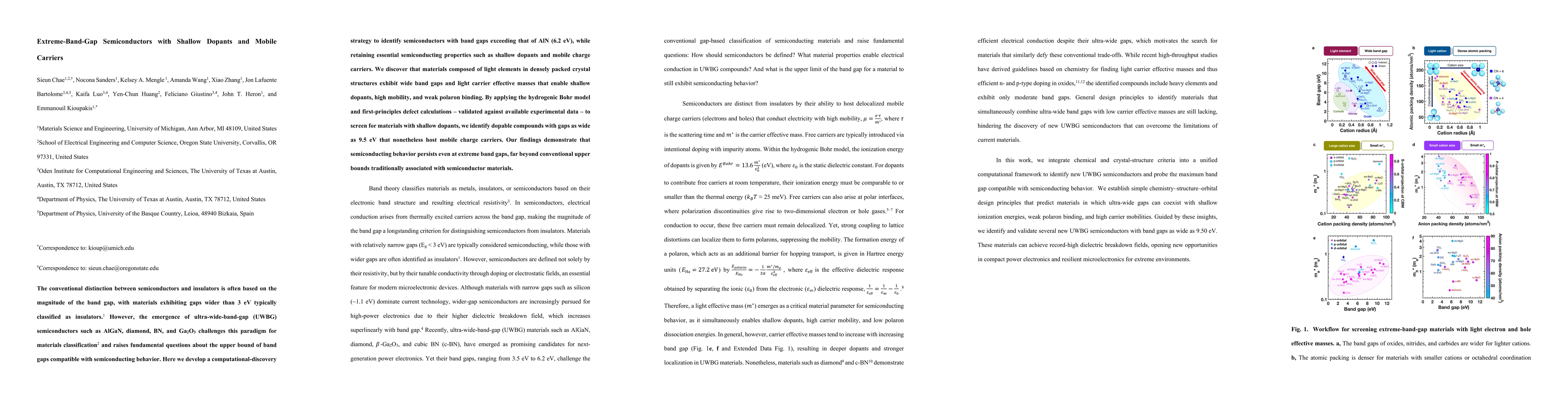
The conventional distinction between semiconductors and insulators is often based on the magnitude of the band gap, with materials exhibiting gaps wider than 3 eV typically classified as insulators. However, the emergence of ultra-wide-band-gap (UWBG) semiconductors such as AlGaN, diamond, BN, and Ga2O3 challenges this paradigm for materials classification and raises fundamental questions about the upper bound of band gaps compatible with semiconducting behavior. Here we develop a computational-discovery strategy to identify semiconductors with band gaps exceeding that of AlN (6.2 eV), while retaining essential semiconducting properties such as shallow dopants and mobile charge carriers. We discover that materials composed of light elements in densely packed crystal structures exhibit wide band gaps and light carrier effective masses that enable shallow dopants, high mobility, and weak polaron binding. By applying the hydrogenic Bohr model and first-principles defect calculations - validated against available experimental data - to screen for materials with shallow dopants, we identify dopable compounds with gaps as wide as 9.5 eV that nonetheless host mobile charge carriers. Our findings demonstrate that semiconducting behavior persists even at extreme band gaps, far beyond conventional upper bounds traditionally associated with semiconductor materials.
AI Key Findings
Get AI-generated insights about this paper's methodology, results, and significance.
Paper Details
PDF Preview
Citation Network
Current paper (gray), citations (green), references (blue)
Display is limited for performance on very large graphs.
Similar Papers
Found 4 papersNo citations found for this paper.
Comments (0)