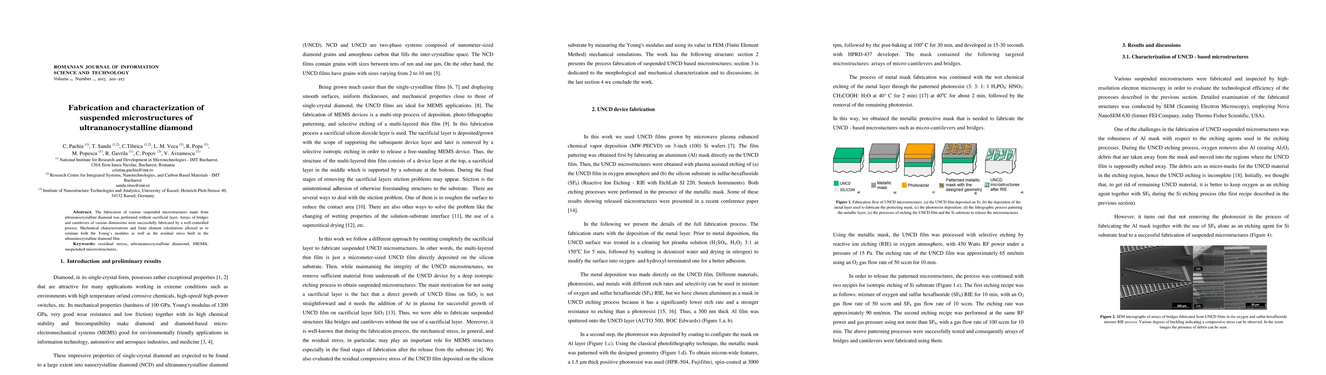
Processing and mechanical characterization of ultrananocrisytalline diamond films for MEMS applications
|
C. Pachiu, C. Tibeica, A. Avram, M. Veca, T. Sandu, M. Popescu, R. Popa
|
2017
|
View Paper
|
High density plasma etching of ultrananocrystalline diamond films in O2/CF4 and O2/SF6 inductively coupled plasmas
|
Jong Cheon Park, S. Kim, T. Kim, Jin Kon Kim, Hyun Cho, B. Lee
|
2015
|
View Paper
|
Surface science, MEMS and NEMS: Progress and opportunities for surface science research performed on, or by, microdevices
|
D. Berman, J. Krim
|
2013
|
View Paper
|
Low temperature growth of nanocrystalline and ultrananocrystalline diamond films: A comparison
|
W. Kulisch, C. Petkov, E. Petkov, C. Popov, P. N. Gibson, M. Veres, R. Merz, B. Merz, J. Reithmaier
|
2012
|
View Paper
|
The mechanical properties of various chemical vapor deposition diamond structures compared to the ideal single crystal
|
P. Hess
|
2012
|
View Paper
|
On the development of the morphology of ultrananocrystalline diamond films
|
W. Kulisch, C. Popov, Takao Sasaki, L. Sirghi, H. Rauscher, F. Rossi, J. Reithmaier
|
2011
|
View Paper
|
Status review of the science and technology of ultrananocrystalline diamond (UNCD™) films and application to multifunctional devices
|
O. Auciello, A. Sumant
|
2010
|
View Paper
|
The CVD of Nanodiamond Materials
|
J. Butler, A. Sumant
|
2008
|
View Paper
|
Diamond and diamond-like carbon MEMS
|
J. K. Luo, Y. Q. Fu, H. Le, J. Williams, S. Spearing, W. I. Milne
|
2007
|
View Paper
|
Materials science and fabrication processes for a new MEMS technology based on ultrananocrystalline diamond thin films
|
O. Auciello, J. Birrell, J. Carlisle, J. Gerbi, Xingcheng Xiao, B. Peng, H. Espinosa
|
2004
|
View Paper
|
Measurement of hardness and elastic modulus by instrumented indentation: Advances in understanding and refinements to methodology
|
W. Oliver, G. Pharr
|
2004
|
View Paper
|
Ultrananocrystalline diamond thin films for MEMS and moving mechanical assembly devices
|
A. Krauss, O. Auciello, D. Gruen, A. Jayatissa, A. Sumant, J. Tucek, D. Mancini, N. Moldovan, A. Erdemir, D. Ersoy, M. Gardos, H. Busmann, E. Meyer, M. Ding
|
2001
|
View Paper
|
Surface Micromachining: A Brief Introduction
|
M. Mehregany, C. Zorman
|
2001
|
View Paper
|
Optical, thermal and mechanical properties of CVD diamond
|
S. Coe, R. Sussmann
|
2000
|
View Paper
|
Effects of elevated temperature treatments in microstructure release procedures
|
T. Abe, W. Messner, M. L. Reed
|
1995
|
View Paper
|
Fabrication and characterisation of suspended microstructures of tantalum
|
A. K. Al-mashaal, E. Mastropaolo, Andrew Bunting, Camelia Dunare, Rebecca Cheung
|
2016
|
View Paper
|
Reactive Ion Etching of 4H-SiC Using SF6/O2 for MEMS Application
|
Y. Hezarjaribi, M. Hamidon
|
2013
|
View Paper
|
Types of Nanocrystalline Diamond
|
O. Shenderova, G. Mcguire
|
2006
|
View Paper
|
Micromachined thin-film sensors for SOI-CMOS co-integration
|
J. Laconte, D. Flandre, J. Raskin
|
2006
|
View Paper
|
Surface roughness modification of interfacial contacts in polysilicon microstructures
|
|
1993
|
|
Supercritical carbon dioxide drying of microstructures
|
|
1993
|
|
Comments (0)