Publication
Metrics
AI Quick Summary
This paper reviews recent advancements in fabricating devices with 2D materials, highlighting various techniques for integrating these materials on chips. It discusses current challenges and future perspectives for achieving high performance and reproducibility in integrated 2D material devices.
Paper Preview
Abstract
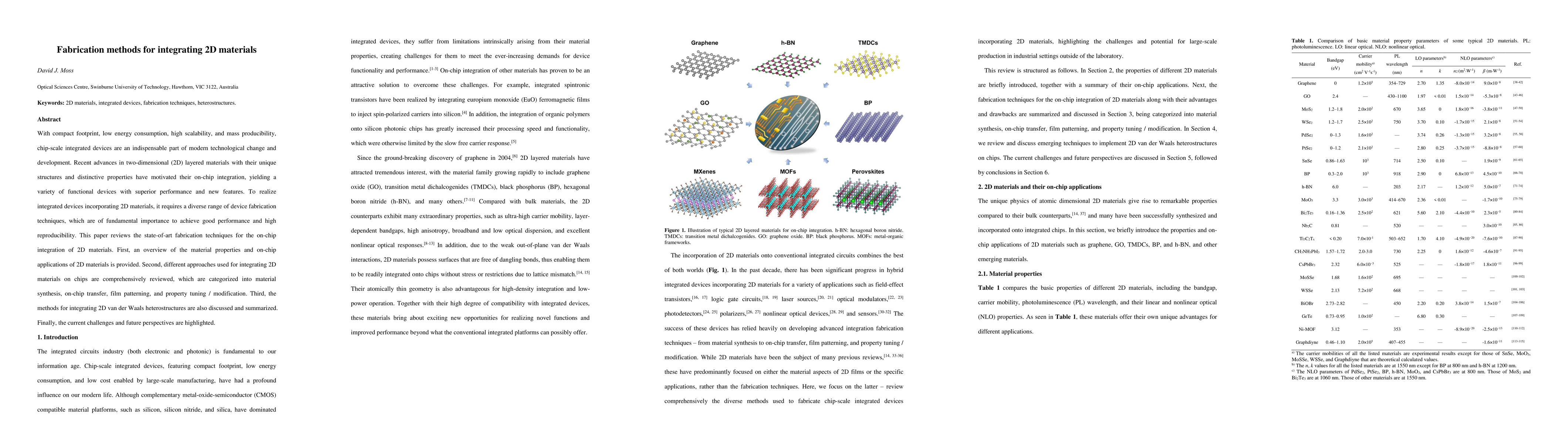
With compact footprint, low energy consumption, high scalability, and mass producibility, chip-scale integrated devices are an indispensable part of modern technological change and development. Recent advances in two-dimensional (2D) layered materials with their unique structures and distinctive properties have motivated their on-chip integration, yielding a variety of functional devices with superior performance and new features. To realize integrated devices incorporating 2D materials, it requires a diverse range of device fabrication techniques, which are of fundamental importance to achieve good performance and high reproducibility. This paper reviews the state-of-art fabrication techniques for the on-chip integration of 2D materials. First, an overview of the material properties and on-chip applications of 2D materials is provided. Second, different approaches used for integrating 2D materials on chips are comprehensively reviewed, which are categorized into material synthesis, on-chip transfer, film patterning, and property tuning / modification. Third, the methods for integrating 2D van der Waals heterostructures are also discussed and summarized. Finally, the current challenges and future perspectives are highlighted.
AI Key Findings
Get AI-generated insights about this paper's methodology, results, significance, and more — seven facets brought into focus.
Impact
Paper Details
Authors
PDF Preview
Key Terms
Citation Network
Current paper (gray), citations (green), references (blue)
Display is limited for performance on very large graphs.
Discussion 0