Summary
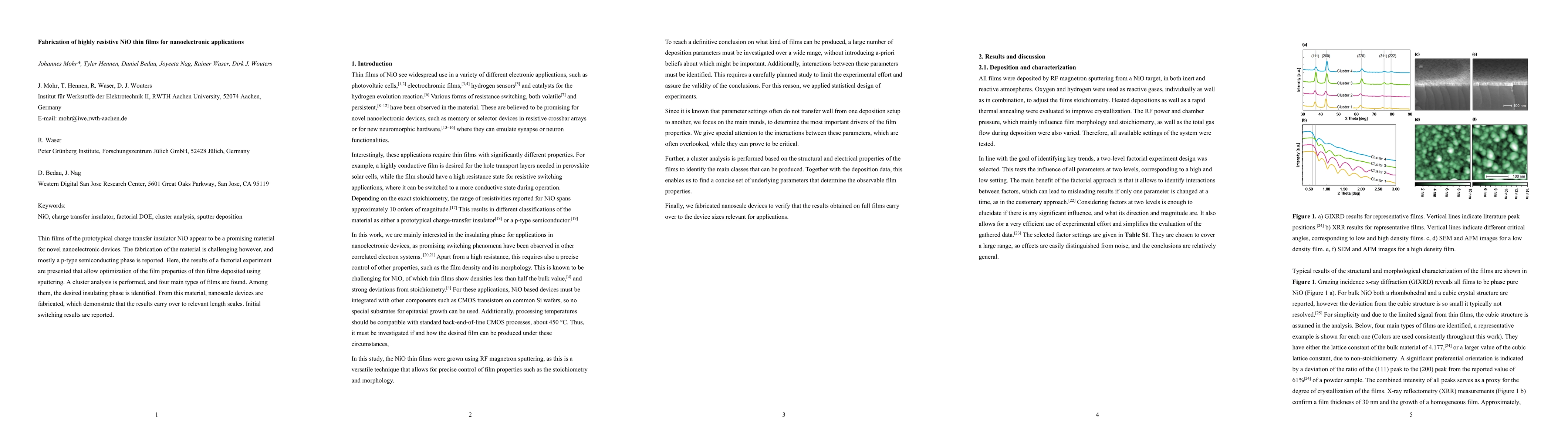
Thin films of the prototypical charge transfer insulator NiO appear to be a promising material for novel nanoelectronic devices. The fabrication of the material is challenging however, and mostly a p-type semiconducting phase is reported. Here, the results of a factorial experiment are presented that allow optimization of the film properties of thin films deposited using sputtering. A cluster analysis is performed, and four main types of films are found. Among them, the desired insulating phase is identified. From this material, nanoscale devices are fabricated, which demonstrate that the results carry over to relevant length scales. Initial switching results are reported.
AI Key Findings
Generated Sep 03, 2025
Methodology
The research utilized a factorial design and linear models for analysis, combined with cluster analysis via k-means algorithm to categorize NiO thin films based on their properties. Sputtering was employed for thin film deposition, with various deposition factors (power, pressure, gas flow, oxygen, hydrogen, deposition temperature, and annealing) systematically varied.
Key Results
- Four main types of NiO thin films were identified, with one type exhibiting the desired insulating phase.
- Film properties such as density, roughness, lattice constant, crystallization, and resistance were found to be influenced by specific deposition factors.
- A post-annealing step was identified as crucial for adjusting stoichiometry and achieving high resistivity in NiO films.
- Nanoscale devices fabricated from the insulating films demonstrated promising resistive switching behavior with low operating currents.
- The study concluded that high-temperature deposition and a post-annealing step are necessary for producing dense, high-resistivity NiO films suitable for nanoelectronic applications.
Significance
This research is significant as it provides a systematic approach to optimize the fabrication of highly resistive NiO thin films, which are crucial for nanoelectronic devices. The findings offer insights into controlling film properties through deposition parameters, enabling the production of NiO thin films with desired characteristics for practical applications.
Technical Contribution
The paper presents a detailed factorial design analysis and cluster analysis to optimize NiO thin film properties for nanoelectronic applications, providing a clear roadmap for fabricating high-resistivity, dense NiO films.
Novelty
This work stands out by combining factorial design with cluster analysis to systematically identify and categorize NiO thin films based on their properties, offering a comprehensive understanding of deposition factors' influence on film characteristics for nanoelectronic devices.
Limitations
- The study was limited to NiO thin films fabricated via sputtering, so the results might not generalize to other deposition techniques.
- The research focused on a specific set of deposition factors; other parameters not investigated could also influence film properties.
- The nanodevices' switching characteristics were only preliminarily investigated, and further detailed studies are needed to understand the switching mechanism fully.
Future Work
- Investigate the impact of alternative deposition methods on NiO thin film properties.
- Explore additional deposition parameters to expand the understanding of their influence on film characteristics.
- Conduct in-depth studies on the resistive switching behavior of NiO nanodevices to optimize their performance for practical applications.
Paper Details
PDF Preview
Key Terms
Citation Network
Current paper (gray), citations (green), references (blue)
Display is limited for performance on very large graphs.
Similar Papers
Found 4 papers| Title | Authors | Year | Actions |
|---|
Comments (0)