Fabrication of photonic nanostructures from hexagonal boron nitride
Publication
Metrics
AI Quick Summary
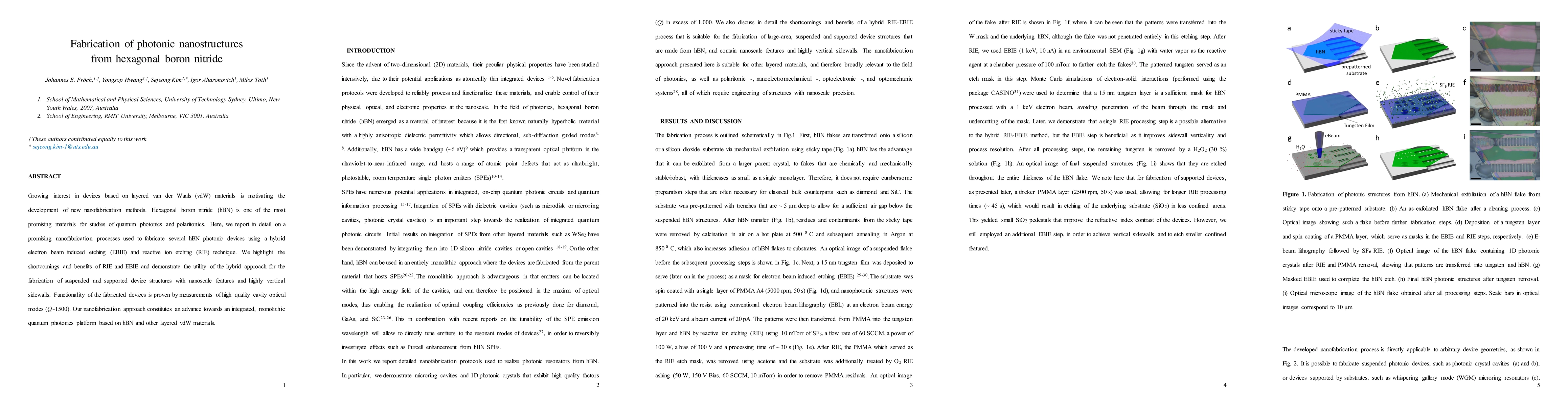
This paper details a hybrid nanofabrication process combining electron beam induced etching (EBIE) and reactive ion etching (RIE) to create photonic devices from hexagonal boron nitride (hBN). The method offers precise, nanoscale structures with vertical sidewalls, demonstrating functional devices with high-quality optical modes (Q~1500).
Paper Preview
Abstract
Growing interest in devices based on layered van der Waals (vdW) materials is motivating the development of new nanofabrication methods. Hexagonal boron nitride (hBN) is one of the most promising materials for studies of quantum photonics and polaritonics. Here, we report in detail on a promising nanofabrication processes used to fabricate several hBN photonic devices using a hybrid electron beam induced etching (EBIE) and reactive ion etching (RIE) technique. We highlight the shortcomings and benefits of RIE and EBIE and demonstrate the utility of the hybrid approach for the fabrication of suspended and supported device structures with nanoscale features and highly vertical sidewalls. Functionality of the fabricated devices is proven by measurements of high quality cavity optical modes (Q~1500). Our nanofabrication approach constitutes an advance towards an integrated, monolithic quantum photonics platform based on hBN and other layered vdW materials.
AI Key Findings
Get AI-generated insights about this paper's methodology, results, significance, and more — seven facets brought into focus.
Impact
Paper Details
PDF Preview
Key Terms
Citation Network
Current paper (gray), citations (green), references (blue)
Display is limited for performance on very large graphs.
Discussion 0